Fpga programming from serial flash memory, Fpga programming from serial flash memory –17 – Altera Stratix V Advanced Systems Development Board User Manual
Page 27
Chapter 2: Board Components
2–17
Configuration, Status, and Setup Elements
January 2014
Altera Corporation
Stratix V Advanced Systems Development Board
Reference Manual
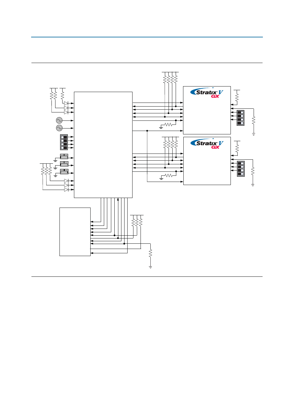
shows the PFL configuration.
f
For more information on the flash memory map storage, refer to the
.
FPGA Programming from Serial Flash Memory
Each FPGA has an EPCQ (serial flash memory) that connects to it’s Active Serial (AS)
configuration pins. On board power-up, each FPGA can be configured via AS x4
mode from the EPCQ device. The contents of the EPCQ devices are written using the
Altera Serial Flash Loader through the Stratix V GX FPGAdevice.
1
To write to the EPCQ device or configure the FPGA via AS x4 mode, the respective
FPGA must have it’s MSEL[4:0] pins set to AS x4 mode.
Figure 2–4. PFL Configuration
MAX V CPLD
System Controller
FPGA_DATA [7:0]
FPGA1_DCLK
F
LA
S
H
_A
[25:1]
F
LA
S
H
_D
[31:0]
FPP Port
DATA [7:0]
DCLK
INIT_DONE
nSTATUS
nCONFIG
CONF_DONE
MSEL0
MSEL1
MSEL2
MSEL3
2.5 V
10 k
Ω
nCE
FPGA1
FPGA2
CFI Flash
1 k
Ω
F
LASH_
C
En
F
LASH_
O
En
F
LASH_
W
En
FLASH_A [25:0]
FLASH_D [15:0]
FLASH_CEn
FLASH_OEn
FLASH_WEn
FLASH_WPn
FLASH_ADVn
FLASH_ADVn
FPGA1_nCONFIG
FPGA1_CONF_DONE
FLASH_RYBSYn
FPGA1_nSTATUS
FPGA1_nCE
ERROR
LOAD
FACTORY
1.8 V
10 k
Ω
2.5 V
F
LA
S
H
_RYBSYn
PGM_SEL
10 k
Ω
FLASH_CLK
F
LA
S
H
_C
LK
F
LASH_
R
ST
n
FLASH_RESETn
50 MHz
100 MHz
PGM_CONFIG
MAX_RESETn
2.5 V
1 k
Ω
1 k
Ω
1 k
Ω
MSEL4
MSEL[4:0] also
connects to MAX V
FPGA1_INIT_DONE
FPGA2_DCLK
FPGA2_nCONFIG
FPGA2_CONF_DONE
FPGA2_nSTATUS
FPGA2_nCE
FPGA2_INIT_DONE
2.5 V
56.2
Ω
CLK_SEL
CLK_ENABLE
USER_PGM
USB_SELECT
DIP Switch
DIP Switch
FPP Port
DATA [7:0]
DCLK
INIT_DONE
nSTATUS
nCONFIG
CONF_DONE
MSEL0
MSEL1
MSEL2
MSEL3
2.5 V
10 k
Ω
nCE
2.5 V
1 k
Ω
1 k
Ω
MSEL4
MSEL[4:0] also
connects to MAX V
DIP Switch
PGM_LED0
PGM_LED1
PGM_LED2
2.5 V
56.2
Ω
10 k
Ω