I/o resources, I/o resources –6 – Altera Stratix V Advanced Systems Development Board User Manual
Page 16
2–6
Chapter 2: Board Components
Featured Device: Stratix V GX FPGA
Stratix V Advanced Systems Development Board
January 2014
Altera Corporation
Reference Manual
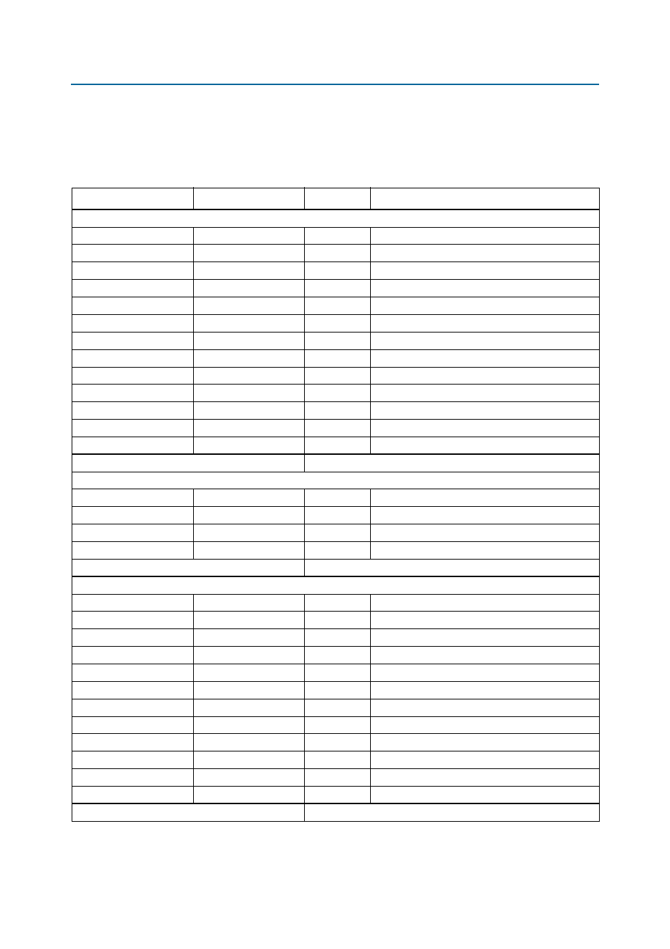
I/O Resources
lists the Stratix V GX FPGA device pin count and usage by function on the
development board.
Table 2–3. Stratix V GX FPGA Pin Count and Usage (Part 1 of 2)
Function
I/O Standard
I/O Count
Special Pins
FPGA1
DDR3
1.5-V SSTL
368
4 differential, 24 differential DQS
QDRII+
1.5-V SSTL
260
4 differential DQS
EEPROM
2.5-V CMOS
2
FMC
Adjustable
80
36 differential, 2 reference clocks
Switches
1.5-V CMOS
8
LEDs
1.5-V/2.5-V CMOS
19
Push buttons
1.5-V/2.5-V CMOS
4
Chip-to-chip
2.5-V CMOS + LVDS
20
4 differential
MAX V Interface
1.5-V/2.5-V CMOS
4
MoSys
1.5-V CMOS
10
PCI Express/PLX
1.5-V/2.5-V CMOS
10
Clocks or Oscillators
1.5-V CMOS + LVDS
26
5 differential clock, 7 differential reference clocks
On-board USB-Blaster II
1.5-V CMOS
19
Total I/O Used:
830
Transceiver Pairs
Chip-to-chip
8
FMC
10
MoSys
16
PCI Express/PLX
8
Total Transceivers Used:
42
FPGA2
DDR3
1.5-V SSTL
368
4 differential, 24 differential DQS
QDRII+
1.5-V SSTL
260
4 differential DQS
EEPROM
2.5-V CMOS
2
HSMC
2.5-V CMOS + LVDS
84
38 differential, 3 clocks
Switches
1.5-V CMOS
8
LEDs
1.5-V CMOS
19
Push-buttons
1.5-V/2.5-V CMOS
4
Chip-to-chip
2.5-V CMOS + LVDS
20
4 differential
MAX V Interface
1.5-V/2.5-V CMOS
4
MoSys
1.5-V CMOS
10
PCI Express/PLX
1.5-V/2.5-V CMOS
6
Clocks or Oscillators
1.5-V CMOS + LVDS
24
5 differential clock, 6 differential reference clocks
Total I/O Used:
809