Temperature sense, Temperature sense –68 – Altera Stratix V Advanced Systems Development Board User Manual
Page 78
2–68
Chapter 2: Board Components
Temperature Sense
Stratix V Advanced Systems Development Board
January 2014
Altera Corporation
Reference Manual
Temperature Sense
Temperature monitoring for both Stratix V GX FPGA dies is achieved with a
MAX1619 temperature sense device. The MAX1619 device connects to the MAX V
CPLD System Controller by a 2-wire SMB interface. The MAX1619 device is located at
address 0x1 for FPGA1 and address 0x2 for FPGA2.
The FPGA1_OVERTEMP and TSENSE_ALERTn_1 signals are driven by the MAX1619
temperature sense device based on a programmable threshold temperature for
FPGA1. The FPGA1_OVERTEMP signal is driven to the MAX V CPLD System Controller
to control FPGA1 fan speed. The FPGA2_OVERTEMP and TSENSE_ALERTn_2 signals are
driven by the MAX1619 temperature sense device based on a programmable
threshold temperature for FPGA2. The FPGA2_OVERTEMP signal is driven to the MAX V
CPLD System Controller to control FPGA2 fan speed.
The MAX V CPLD System Controller can control fan speed for each FPGA based on a
register setting and can also override the MAX1619 device. For more information
about this control, refer to the MAX V CPLD System Controller source code found in
the development board installation directory
<install dir>\stratixVGX_5sgxea7nf45_as\examples\max5
f
For more information on the development board installation directory, refer to the
.
The remote sense routes to the FPGA's diode pins to measure the voltage drop. For
very accurate temperature readings, the I/O adjacent to the FPGA diode sense pins
must be halted.
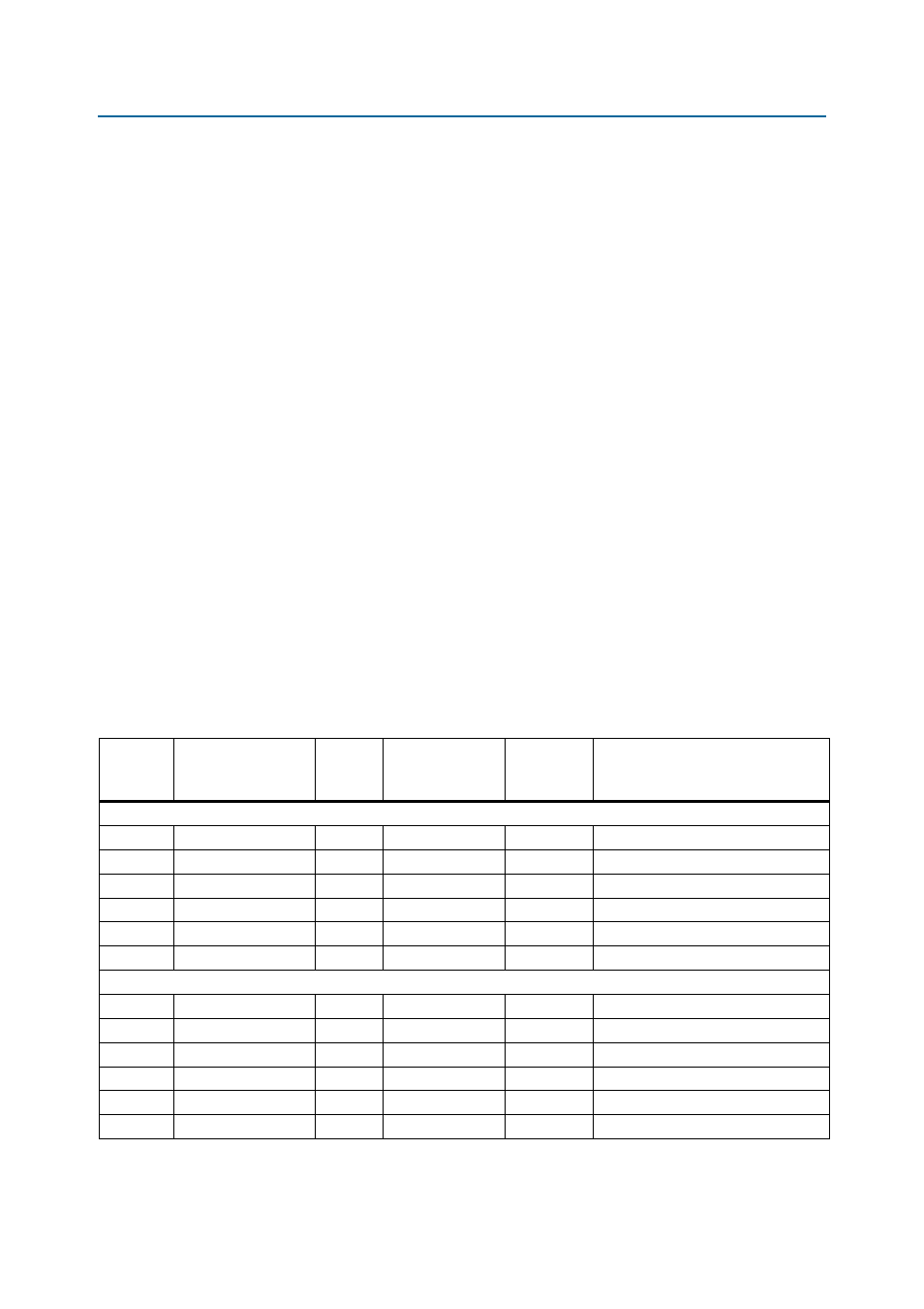
lists the temperature sense interface pin assignments, signal names, and
functions.
Table 2–31. Temperature Sense Pin Assignments, Schematic Signal Names, and Functions
Board
Reference
Schematic Signal
Name
I/O
Standard
MAX V CPLD
System Controller
Pin Number
Stratix V GX
FPGA Device
Pin Number
Description
FPGA1 MAX1619 (U102)
14
SENSE_SMB_CLK
2.5-V
E7
—
SMB clock
12
SENSE_SMB_DATA
2.5-V
E6
—
SMB data
11
TSENSE_ALERTn_1
2.5-V
D8
—
Programmable over temperature alert
9
FPGA1_OVERTEMPn
2.5-V
D7
—
Fan enable
3
FPGA1_TEMPDIODE_P
2.5-V
—
P6
Current source and remote diode input
4
FPGA1_TEMPDIODE_N
2.5-V
—
P7
Remote diode input
FPGA2 MAX1619 (U103)
14
SENSE_SMB_CLK
2.5-V
E7
—
SMB clock
12
SENSE_SMB_DATA
2.5-V
E6
—
SMB data
11
TSENSE_ALERTn_2
2.5-V
B5
—
Programmable over temperature alert
9
FPGA2_OVERTEMPn
2.5-V
E10
—
Fan enable
3
FPGA2_TEMPDIODE_P
2.5-V
—
P6
Current source and remote diode input
4
FPGA2_TEMPDIODE_N
2.5-V
—
P7
Remote diode input