Altera Stratix V Advanced Systems Development Board User Manual
Page 58
2–48
Chapter 2: Board Components
Memory
Stratix V Advanced Systems Development Board
January 2014
Altera Corporation
Reference Manual
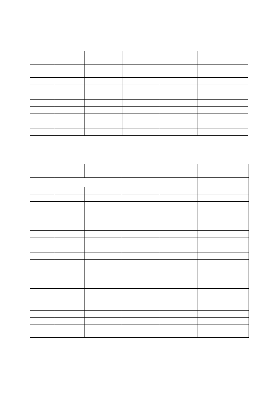
lists the DDR3 devices pin assignments, signal names, and functions for
FPGA2.
B7
DQS_N7
Differential 1.5-V
SSTL Class I
BD28
D15
Data strobe
K1
ODT
1.5-V SSTL Class I
AE31
R18
On-die termination enable
J3
RASN
1.5-V SSTL Class I
AF31
G17
Row address strobe
T2
RESETN
1.5-V SSTL Class I
AE34
A19
Reset
L3
WEN
1.5-V SSTL Class I
AP33
F17
Write enable
L8
ZQ01
—
—
—
ZQ impedance calibration
L8
ZQ02
—
—
—
ZQ impedance calibration
L8
ZQ03
—
—
—
ZQ impedance calibration
L8
ZQ04
—
—
—
ZQ impedance calibration
Table 2–23. FPGA1 DDR3 Devices Pin Assignments, Schematic Signal Names, and Functions (Part 7 of 7)
Board
Reference
Schematic
Signal Name
I/O Standard
Stratix V GX FPGA1 Device Pin Number
Description
Table 2–24. FPGA2 DDR3 Devices Pin Assignments, Schematic Signal Names, and Functions (Part 1 of 6)
Board
Reference
Schematic
Signal Name
I/O Standard
Stratix V GX FPGA2 Device Pin Number
Description
DDR3E_
/ DDR3G_ (x32 bit interface)
DDR3E
DDR3G
N3
A0
1.5-V SSTL Class I
AW20
G28
Address bus
P7
A1
1.5-V SSTL Class I
AT21
G26
Address bus
P3
A2
1.5-V SSTL Class I
BD20
F26
Address bus
N2
A3
1.5-V SSTL Class I
BB20
D29
Address bus
P8
A4
1.5-V SSTL Class I
AU20
A26
Address bus
P2
A5
1.5-V SSTL Class I
BC20
C27
Address bus
R8
A6
1.5-V SSTL Class I
AU21
C28
Address bus
R2
A7
1.5-V SSTL Class I
BA22
B28
Address bus
T8
A8
1.5-V SSTL Class I
BD22
A28
Address bus
R3
A9
1.5-V SSTL Class I
BB21
E27
Address bus
L7
A10
1.5-V SSTL Class I
AY21
H27
Address bus
R7
A11
1.5-V SSTL Class I
AW21
F28
Address bus
N7
A12
1.5-V SSTL Class I
AV20
H28
Address bus
T3
A13
1.5-V SSTL Class I
BC22
D27
Address bus
M2
BA0
1.5-V SSTL Class I
AU22
F29
Bank address bus
N8
BA1
1.5-V SSTL Class I
AT20
B26
Bank address bus
M3
BA2
1.5-V SSTL Class I
BA21
T27
Bank address bus
K3
CASN
1.5-V SSTL Class I
AR21
K28
Column address strobe
K9
CKE
1.5-V SSTL Class I
AP21
G29
Clock enable
K7
CLK_N
Differential 1.5-V
SSTL Class I
AW22
H26
Differential output clock