Featured device: stratix v gx fpga, Featured device: stratix v gx fpga –5 – Altera Stratix V Advanced Systems Development Board User Manual
Page 15
Chapter 2: Board Components
2–5
Featured Device: Stratix V GX FPGA
January 2014
Altera Corporation
Stratix V Advanced Systems Development Board
Reference Manual
Featured Device: Stratix V GX FPGA
The Stratix V Advanced Systems development board features two Stratix V GX FPGA
5SGXEA7N2F45C2N devices (U29, U35) in a 1932-pin FineLine BGA package.
f
For more information about the Stratix V device family, refer to
Table 2–2
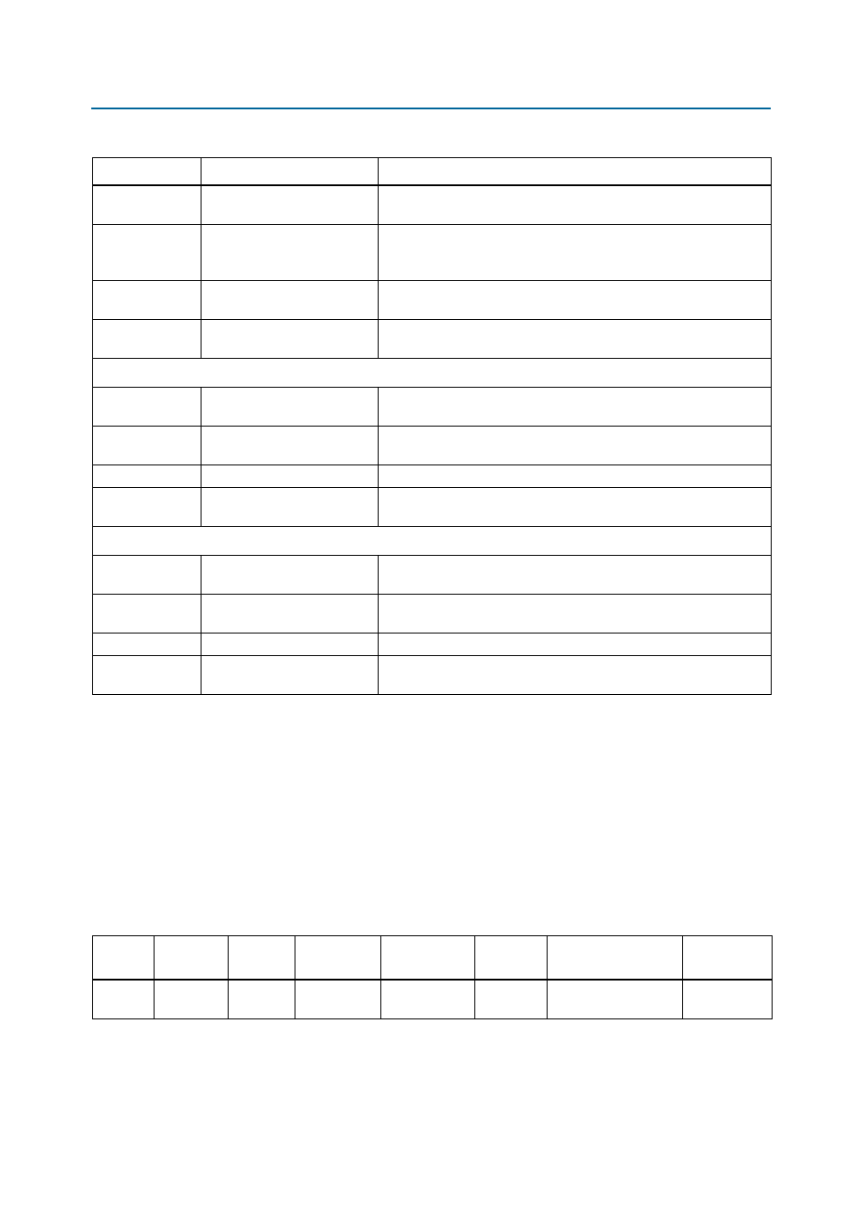
describes the features of the Stratix V GX FPGA 5SGXEA7N2F45C2N
device.
U14
MoSys x16
A 72-MB MoSys Bandwidth Engine IC SRAM with a 16-bit transceiver
data bus for FPGA2.
U86
Flash x16
A 1-Gb synchronous flash device with a 16-bit data bus for non-volatile
memory. Only accessible from the MAX V System Controller, intended
for FPGA configuration.
U93, U48
EPCQ x4
A 32-MB serial flash is available for each FPGA to use during active
serial (AS) configuration.
U76, U83
EEPROM
A single 8-Kbit serial EEPROM is available for each FPGA to store
board information.
Communication Ports
J13
PCI Express edge connector
Made of gold-plated edge fingers for up to ×16 signaling in either
Gen1, Gen2, or Gen3 mode.
U47
PLX PCI Express switch
Switch x16 PCI Express data between FPGA1 x8 and FPGA2 x8 via the
PEX8747 PCIe switch.
J8
FMC port
Provides 10 transceiver channels and 74 CMOS or 17 LVDS channels.
J1
HSMC port
Provides eight transceiver channels and 84 CMOS or 17 LVDS
channels.
Power Supply
J13
PCI Express edge connector
Interfaces to a PCI Express root port such as an appropriate PC
motherboard.
J10
PCI Express 2x4 ATX power
PCI Express compliant 2x4 auxiliary power connector. This can supply
an additional 150 W to the board.
J7
DC input jack
Accepts a 12- to 15-V DC power supply.
SW2
Power switch
Switch to power on or off the board when power is supplied from the
DC input jack.
Table 2–1. Stratix V Advanced Systems Development Board Components (Part 4 of 4)
Board Reference
Type
Description
Table 2–2. Stratix V GX FPGA 5SGXEA7N2F45C2N Features
ALMs
Equivalent
LEs
Registers
M20K
Memory (Mb)
18-bit × 18-bit
Multipliers
Fractional
PLLs
Transceiver Channels
(12.5 Gbps)
Package Type
358,500
622,000
939,000
50
512
28
48
1932-pin
FineLine BGA