Altera Stratix V Advanced Systems Development Board User Manual
Page 21
Chapter 2: Board Components
2–11
MAX V CPLD System Controller
January 2014
Altera Corporation
Stratix V Advanced Systems Development Board
Reference Manual
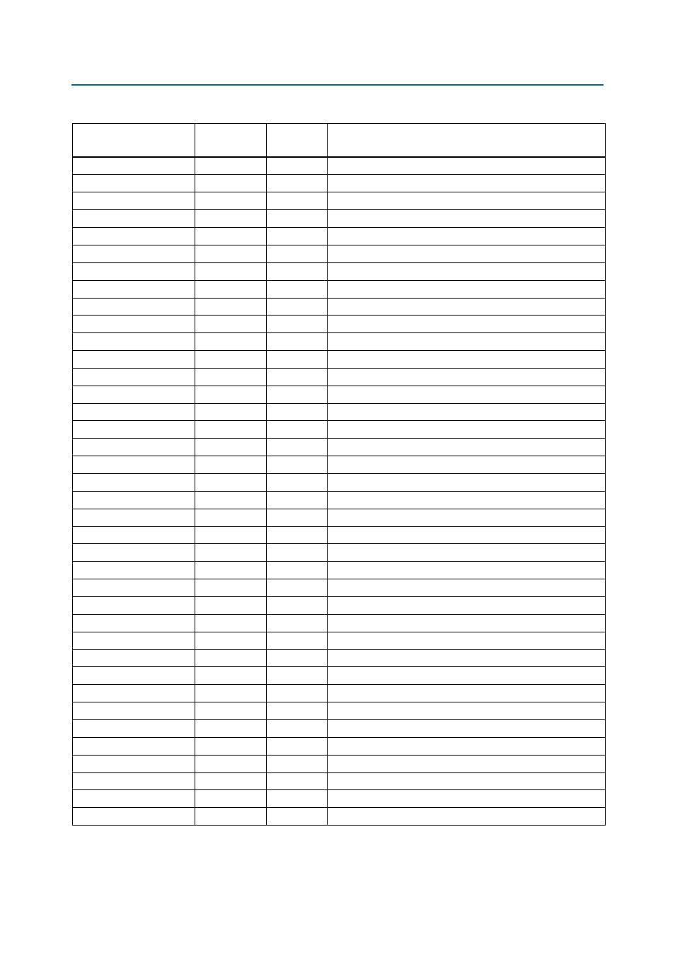
M570_CLOCK
P11
1.5-V
25-MHz clock to on-board USB-Blaster II
M570_PCIE_JTAG_EN
E11
2.5-V
Reserved
MAX5_CLK
T11
1.5-V
MAX V clock
MAX5_DATA
P5
1.5-V
MAX V data
MAX_CONF_DONE
C11
2.5-V
FPGA configuration done LED
MAX_ERROR
A9
2.5-V
FPGA configuration error LED
MAX_LOAD
B12
2.5-V
FPGA configuration active LED
MAX_RESETN
M9
1.5-V
MAX V reset push button
MV_CLK_50
J12
1.8-V
50-MHz clock input
PGM_CONFIG
D9
2.5-V
Loads the flash memory image identified by the PGM LEDs
PGM_LED0
B9
2.5-V
Flash memory PGM select indicator 0
PGM_LED1
C10
2.5-V
Flash memory PGM select indicator 1
PGM_LED2
D12
2.5-V
Flash memory PGM select indicator 2
PGM_SEL
C9
2.5-V
Toggles the PGM_LED[0:2] sequence
SENSE_CS0N
C12
2.5-V
Power monitor chip select
SENSE_SCK
B6
2.5-V
Power monitor SPI clock
SENSE_SDI
B11
2.5-V
Power monitor SPI data in
SENSE_SDO
B10
2.5-V
Power monitor SPI data out
SENSE_SMB_CLK
E7
2.5-V
Temperature monitor SMB clock
SENSE_SMB_DATA
E6
2.5-V
Temperature monitor SMB data
SI53154_SCLK
C8
2.5-V
Si53154 serial clock
SI53154_SDATA
A10
2.5-V
Si53154 serial data
TSENSE_ALERTN_1
D8
2.5-V
FPGA1 temperature monitor alert
TSENSE_ALERTN_2
B5
2.5-V
FPGA2 temperature monitor alert
USB_CFG0
P8
1.5-V
On-board USB Blaster II configuration
USB_CFG1
N6
1.5-V
On-board USB Blaster II configuration
USB_CFG2
M6
1.5-V
On-board USB Blaster II configuration
USB_CFG3
M7
1.5-V
On-board USB Blaster II configuration
USB_CFG4
N8
1.5-V
On-board USB Blaster II configuration
USB_CFG5
N7
1.5-V
On-board USB Blaster II configuration
USB_CFG6
P9
1.5-V
On-board USB Blaster II configuration
USB_CFG7
N11
1.5-V
On-board USB Blaster II configuration
USB_CFG8
T9
1.5-V
On-board USB Blaster II configuration
USB_CFG9
T10
1.5-V
On-board USB Blaster II configuration
USB_CFG10
R9
1.5-V
On-board USB Blaster II configuration
USB_CFG11
T8
1.5-V
On-board USB Blaster II configuration
USB_CFG12
R16
1.5-V
On-board USB Blaster II configuration
USB_CFG13
T13
1.5-V
On-board USB Blaster II configuration
Table 2–4. MAX V CPLD System Controller Device Pin-Out (Part 4 of 5)
Schematic Signal Name
MAX V CPLD
Pin Number
I/O
Standard
Description