3 hpa, ps, u/c, and d/c, j3 db37-male – Comtech EF Data CST-5000 User Manual
Page 96
CST-5000 C-Band Satellite Terminal
Theory of Operation
Rev. 9
5–7
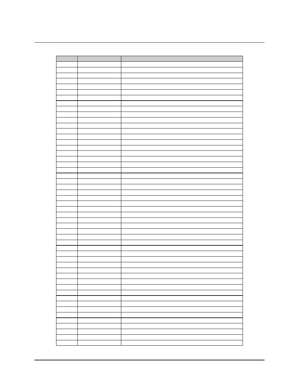
5.1.5.3 HPA, PS, U/C, and D/C, J3 DB37-Male
Pin #
Name
Description
1
12.5V PWR
Input power to M&C, 12.5V, 220 mA
20
12.5V PWR
Input power to M&C, 12.5V, 220 mA
2
DC LNA PWR
Output power to DC, 10V, 100 mA
21 GND
M&C
ground
3 GND
M&C
ground
22
FAN TACH
Input pulse, 0 to 12V, 9 millisecond period
4
FREQ CNTRL
Output, voltage 0 to 10V
23
FAN CNTRL
Output, NPN OC Transistor with resistor to 5V
5 SPARE
24
EXT OUTPUT1
Output, digital CMOS level - function TBD
6
EXT INPUT3
Input, digital CMOS - function TBD
25
HPA FLT COM
Output, ground connection to relay common
7
HPA FLT NO
Input from HPA, contact to COM during normal operation
26 SPARE
8 SPARE
27
HPA THERM
Input, 5K thermistor to ground located in HPA
9
HPA LEVEL CON
Output, 0 to 4 VDC for AGC control of HPA output
28
HPA SHUTDOWN
Output, NPN OC transistor to GND, low produces shut-off
10
HPA PWR MON
Input from HPA, 0 to 4V
29 SPARE
11 SPARE
30 SPARE
12
DC LEVEL CON
Output, analog voltage 0 to 4V, AGC control of D/C output
31
DC LEVEL MON
Input, 0 to 4V
13
DC THERM
Input, 5K thermistor to ground located in D/C
32 SPARE
14
HPA SDA
Bi-directional serial data
33
DC SDA
Bi-directional serial data
15
UC SDA
Bi-directional serial data
34
HPA SCL
Output, serial clock
16
DC SCL
Output, serial clock
35
UC SCL
Output, serial clock
17 SPARE
36
UC LEVEL MON
Input, 0 to 4V
18
UC THERM
Input, 5K thermistor to ground located in U/C
37
UC ATT (FLC)
Output, analog voltage 0 to 4V, attenuator control
19
UC AGC (CLC)
Output, analog voltage 0 to 4V, AGC control