4 synthesizers (dc/uc/lo), j4 db37-female – Comtech EF Data CST-5000 User Manual
Page 97
Theory of Operation
CST-5000 C-Band Satellite Terminal
5–8
Rev. 9
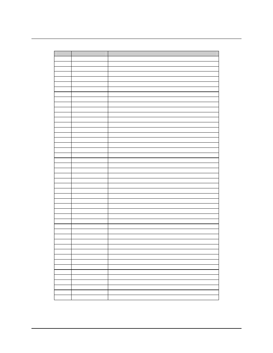
5.1.5.4 Synthesizers (DC/UC/LO), J4 DB37-Female
Pin #
Name
Description
1
UC LO A0
Output CMOS level, LSB
(selects the 2nd
20
UC LO A1
Output CMOS level, 2LSB
divide-by number)
2
UC LO A2
Output CMOS level, 2MSB
21
UC LO A3
Output CMOS level, MSB
3
UC LO G0
Output CMOS level, LSB
(selects gain over
22
UC LO G1
Output CMOS level, 2LSB
frequency)
4
UC LO G2
Output CMOS level, 2MSB
23
UC LO G3
Output CMOS level, MSB
5
UC LO N0
Output CMOS level, LSB
(selects the first
24
UC LO N1
Output CMOS level, 2LSB
divide-by number
6
UC LO N2
Output CMOS level, 3LSB
in the synthesizer)
25
UC LO N3
Output CMOS level, 3MSB
7
UC LO N4
Output CMOS level, 2MSB
26
UC LO N5
Output CMOS level, MSB
8
DC LO LCK DET
Input, 0V = locked, 5V = unlocked
27
DC LO T_MON
Input, 0 to 11V, nominal reading = 6V
9 SPARE
28 SPARE
10
IF LCK DET
Input, 0V = locked, 5V = unlocked
29
IF T_MON
Input, 0 to 11V, nominal reading = 6V
11 SPARE
30
DC LO A0
Output CMOS level, LSB
(selects the 2nd
12
DC LO A1
Output CMOS level, 2LSB
divide-by number)
31
DC LO A2
Output CMOS level, 2MSB
13
DC LO A3
Output CMOS level, MSB
32
DC LO G0
Output CMOS level, LSB
(selects gain
14
DC LO G1
Output CMOS level, 2LSB
over frequency)
33
DC LO G2
Output CMOS level, 2MSB
15
DC LO G3
Output CMOS level, MSB
34
DC LO N0
Output CMOS level, LSB
(selects the first
16
DC LO N1
Output CMOS level, 2LSB
divide by number
35
DC LO N2
Output CMOS level, 3LSB
in the synthesizer)
17
DC LO N3
Output CMOS level, 3MSB
36
DC LO N4
Output CMOS level, 2MSB
18
DC LO N5
Output CMOS level, MSB
37
UC LO LCK DET
Input, 0V = locked, 5V = unlocked
19
UC LO T_MON
Input, 0 to 11V, nominal reading = 6V