Configuration space register access – Altera Arria V Avalon-MM User Manual
Page 51
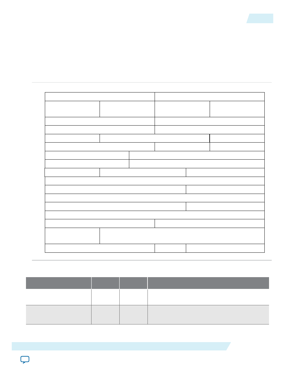
Configuration Space Register Access
The
tl_cfg_ctl
signal is a multiplexed bus that contains the contents of Configuration Space registers as
shown in the figure below. Information stored in the Configuration Space is accessed in round robin
order where
tl_cfg_add
indicates which register is being accessed. The following table shows the layout
of configuration information that is multiplexed on
tl_cfg_ctl
.
Figure 4-6: Multiplexed Configuration Register Information Available on tl_cfg_ctl
Fields in blue are available only for Root Ports.
0
1
cfg_dev_ctrl[15:0]
31
24 23
16 15
8 7
0
2
3
4
5
6
7
8
9
A
B
C
D
E
F
cfg_dev_ctrl2[15:0]
cfg_link_ctrl[15:0]
cfg_link_ctrl2[15:0]
cfg_dev_ctrl[14:12] =
Max Read Req Size
16’h0000
cfg_slot_ctrl[15:0]
8’h00
cfg_root_ctrl[7:0]
cfg_secbus[7:0]
cfg_subbus[7:0]
cfg_sec_ctrl[15:0]
cfg_msi_addr[11:0]
cfg_io_bas[19:0]
cfg_dev_ctrl[7:5] =
Max Payload
cfg_pgm_cmd[15:0]
cfg_msi_addr[43:32]
cfg_io_lim[19:0]
8’h00
cfg_np_bas[11:0]
cfg_np_lim[11:0]
cfg_msi_addr[31:12]
cfg_pr_bas[43:32]
cfg_pr_bas[31:0]
cfg_msi_addr[63:44]
cfg_pr_lim[43:32]
cfg_pr_lim[31:0]
cfg_msixcsr[15:09]
cfg_msicsr[15:0]
cfg_pmcsr[31:0]
6’h00, tx_ecrcgen[25],
rx_ecrccheck[24]
cfg_tcvcmap[23:0]
cfg_msi_data[15:0]
3’b00 0
cfg_busdev[12:0]
Table 4-12: Configuration Space Register Descriptions
Register
Width
Direction
Description
cfg_dev_ctrl_func<n>
16
Output
cfg_dev_ctrl_func<n>[15:0]
is Device Control
register for the PCI Express capability structure.
cfg_dev_ctrl2
16
Output
cfg_dev2ctrl[15:0]
is Device Control 2 for the
PCI Express capability structure.
UG-01105_avmm
2014.12.15
Configuration Space Register Access
4-21
Interfaces and Signal Descriptions
Altera Corporation