Board overview, Board overview –2, Figure 2–1 – Altera 100G Development Kit, Stratix V GX Edition User Manual
Page 10: Table 2–1
2–2
Chapter 2: Board Components
Board Overview
100G Development Kit, Stratix V GX Edition
August 2012
Altera Corporation
Reference Manual
Board Overview
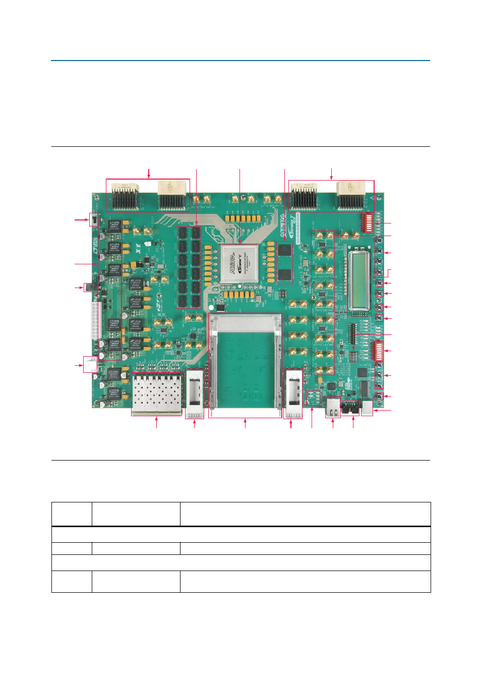
This section provides an overview of the Stratix V GX 100G development board,
including an annotated board image and component descriptions.
provides an overview of the board features.
describes the components and lists their corresponding board references.
Figure 2–1. Overview of the Stratix V GX 100G Development Board Features
Power
Switch
(SW1)
DC Power
Jack (J1)
Character
LCD (J62)
Power
Regulators
Board Settings
DIP Switch (SW4)
DDR3 Memory
(U72-U83)
User DIP Switch
(SW6)
Interlaken Channel 0-11
(J52, J53)
Ethernet
Status LEDs
(D12-D17)
USB Type-B
Connector
(J65)
Stratix V GX FPGA
(U38)
Ethernet
RJ-45
Connector
(J7)
User Push Buttons
(S4-S6)
FPGA User
Push Buttons
(S7-S10)
User DIP Switch
(SW5)
JTAG
Programming
Header
(J59)
Interlaken Channel 12-23
(J54, J55)
QDR II SRAM
(U70, U71)
Clock Circuitry
Auxiliary
Power
Jack (J2)
SFP Connectors (J45)
QSFP
Interface
(J65)
QSFP
Interface
(J67)
CFP
(J46)
CPU Reset
Push Button (S3)
Factory Push Button
(S15)
Load Push Button
(S14)
Reset Push Button
(S1)
Program Select
Push Button (S13)
Table 2–1. Stratix V GX 100G Development Board Components (Part 1 of 4)
Board
Reference
Type
Description
Featured Device
U38
FPGA
5SGXEA7N2F45C2N Stratix V GX device in a 1932-pin FBGA package.
Configuration, Status, and Setup Elements
D24–D29,
D31–D34
Configuration status LEDs
Indicates the FPP configuration status.