Altera 100G Development Kit, Stratix V GX Edition User Manual
Page 23
Chapter 2: Board Components
2–15
MAX II CPLD EPM2210 System Controller
August 2012
Altera Corporation
100G Development Kit, Stratix V GX Edition
Reference Manual
G5
LCD_DATA2
2.5-V
AV11
LCD data
H3
LCD_DATA3
2.5-V
AF31
LCD data
G4
LCD_DATA4
2.5-V
AE12
LCD data
G1
LCD_DATA5
2.5-V
BD20
LCD data
F6
LCD_DATA6
2.5-V
AP31
LCD data
G2
LCD_DATA7
2.5-V
AU11
LCD data
J3
LCD_WEN
2.5-V
AM32
LCD write enable
N17
LINE_SIDE0
2.5-V
—
Spare I/Os on the MAX II CPLD and function as an I/O
expander for the FPGA. Data can pass through the MAX II
CPLD to the Stratix V GX interface.
M13
LINE_SIDE1
2.5-V
—
N18
LINE_SIDE2
2.5-V
—
M12
LINE_SIDE3
2.5-V
—
M16
LINE_SIDE4
2.5-V
—
L16
LINE_SIDE5
2.5-V
—
M17
LINE_SIDE6
2.5-V
—
L15
LINE_SIDE7
2.5-V
—
M18
LINE_SIDE8
2.5-V
—
L14
LINE_SIDE9
2.5-V
—
M5
LOAD
2.5-V
—
Initiates a load of the selected image from the PFL
U16
M570_CLOCK
1.5-V
—
25-MHz clock to on-board USB-Blaster II for sending the
FACTORY command
G12
MAX2_CLK
2.5-V
AW10
MAX II CPLD clock
F17
MAX2_CSN
2.5-V
AG10
MAX II CPLD chip select
F18
MAX2_OEN
2.5-V
AY37
MAX II CPLD output enable
G13
MAX2_WEN
2.5-V
AN12
MAX II CPLD write enable
T16
MAX_CONF_DONEN
2.5-V
—
FPGA configuration done LED. Indicates that the FPGA is
loaded with the new image.
T17
MAX_ERROR
2.5-V
—
FPGA configuration error LED
R15
MAX_LOAD
2.5-V
—
FPGA configuration active LED
C17
OVERTEMPN
2.5-V
—
Over-temperature indicator from the temperature sense
circuit
N1
PGM_SEL
2.5-V
—
Push button to select which image to program into the
FPGA
P3
PHASE60
2.5-V
—
Switch control for the dual 1.5-V and 3.3-V regulators
P2
PHASE120
2.5-V
—
Switch control for the dual 5.0-V and 2.5-V regulators
P4
PHASE180
2.5-V
—
Switch control for the dual 5.0-V and 2.5-V regulators
P1
PHASE240
2.5-V
—
Switch control for the dual 1.5-V and 3.3-V regulators
N4
PWR_CTL
2.5-V
—
Power monitor control
H5
SENSE_CE0
2.5-V
—
Chip select for the first current sense ADC
J2
SENSE_CE1
2.5-V
—
Chip select for the second current sense ADC
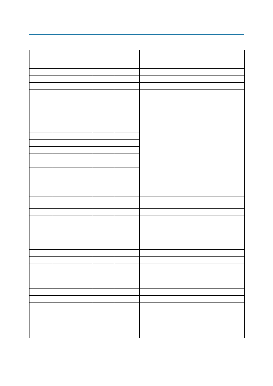
Table 2–5. MAX II CPLD EPM2210 System Controller Device Pin-Out (Part 4 of 5)
Board
Reference
(U59)
Schematic Signal
Name
I/O
Standard
Stratix V GX
Device Pin
Number
Pin Description