Flash memory, Flash memory –30, Table 2–23 – Altera 100G Development Kit, Stratix V GX Edition User Manual
Page 38
2–30
Chapter 2: Board Components
Flash Memory
100G Development Kit, Stratix V GX Edition
August 2012
Altera Corporation
Reference Manual
shows the LCD pin definitions, and is an excerpt from the Lumex data
sheet.
f
For more information such as timing, character maps, interface guidelines, and other
related documentation, visi
1
The particular model used on this board does not have a backlight and therefore the
LCD drive pin is not connected.
lists the LCD component references and the manufacturing information.
Flash Memory
The board features a Numonyx PC28F00AP30BF 1-Gb CFI-compliant NOR-type flash
memory device, which stores configuration files for the FPGA. Both the MAX II CPLD
(U59) and FPGA (U38) devices can access the flash. The MAX II access to the flash’s
user space for FPP configuration of the FPGA using the PFL Megafunction. The FPGA
access to the flash’s user space for embedded NIOS applications.
provides the pin-out information of the flash memory interface to the
FPGA. The signal direction is with respect to the FPGA device.
Table 2–22. LCD Pin Definitions and Functions
Pin Number
Symbol
Level
Function
1
V
DD
—
Power supply
5 V
2
V
SS
—
GND (0 V)
3
V
0
—
For LCD drive
4
RS
H/L
Register select signal
H: Data input
L: Instruction input
5
R/W
H/L
H: Data read (module to MPU)
L: Data write (MPU to module)
6
E
H, H to L
Enable
7–14
DB0–DB7
H/L
Data bus, software selectable 4-bit or 8-bit mode
Table 2–23. LCD Component References And The Manufacturing Information
Board
Reference
Device Description
Manufacturer
Manufacturer
Part Number
Manufacturer
Website
J64
2×16 character display, 5×8 dot matrix
Lumex Inc.
LCM-S01602DSR/C
2×7 pin, 100 mil, vertical header
Samtec
TSM-107-01-G-DV
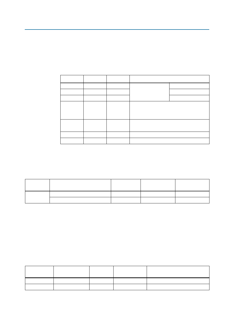
Table 2–24. Flash Memory Pin Assignments, Schematic Signal Names, and Functions (Part 1 of 3)
Board
Reference (U60)
Schematic Signal
Name
I/O Standard
Stratix V GX Device
Pin Number
Description
F6
FLASH_ADVN
2.5-V CMOS
AE34
Flash address valid
B4
FLASH_CEN
2.5-V CMOS
AD14
Flash chip enable