Altera 100G Development Kit, Stratix V GX Edition User Manual
Page 42
2–34
Chapter 2: Board Components
Components and Interfaces
100G Development Kit, Stratix V GX Edition
August 2012
Altera Corporation
Reference Manual
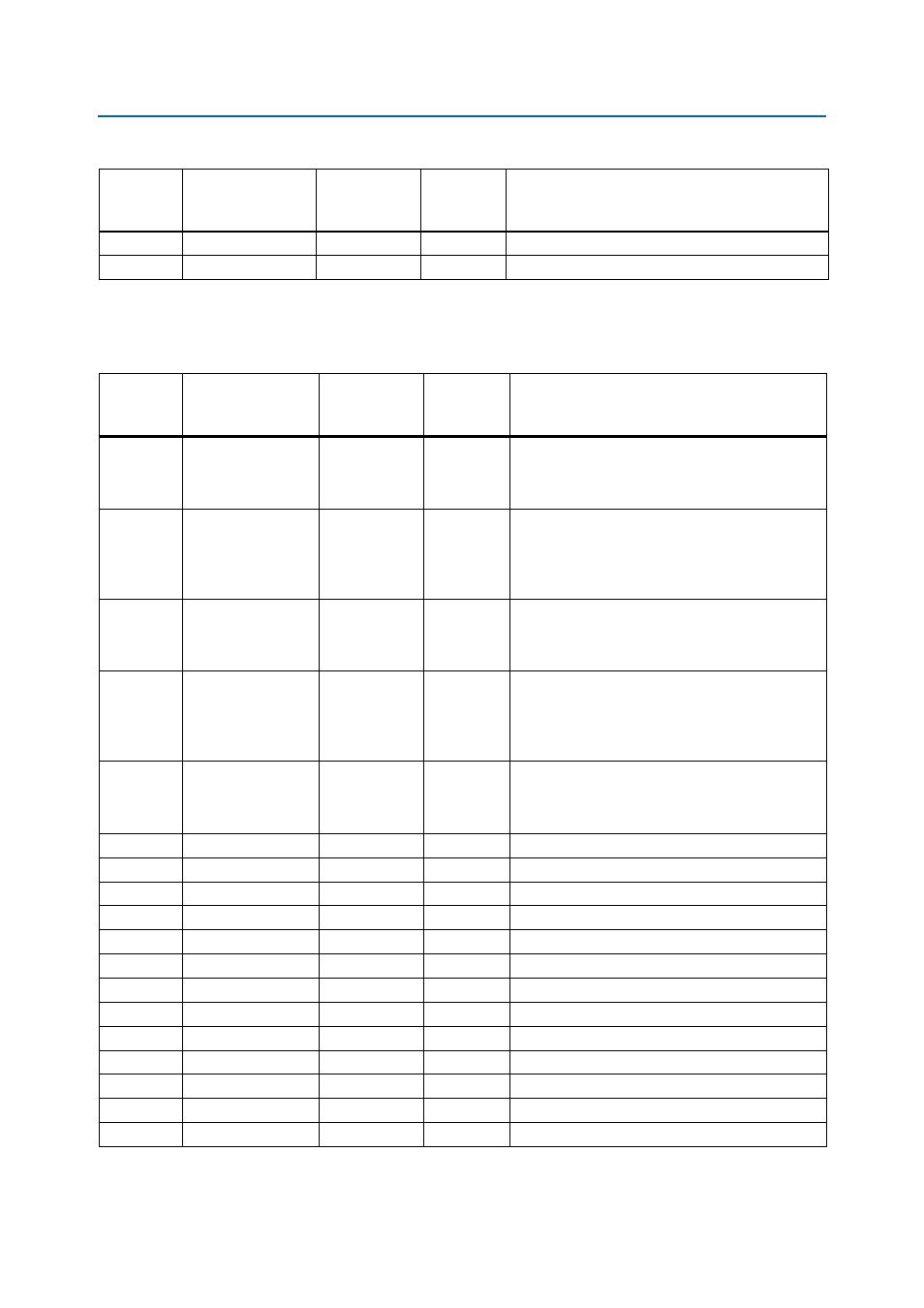
lists the pin assignments for the second QSFP interface (J19) and their
corresponding schematic signal names and Stratix V GX pin numbers.
6
QSFP0_TX_P3
1.5-V PCML
AN4
Transmit XCVR pair 3 from FPGA
5
QSFP0_TX_N3
1.5-V PCML
AN3
Transmit XCVR pair 3 from FPGA
Table 2–26. QSFP Interface Pin Assignments, Schematic Signal Names, and Functions (Part 2 of 2)
Board
Reference
(J33)
Schematic Signal
Name
I/O Standard
Stratix V GX
Device Pin
Number
Description
Table 2–27. QSFP Interface Pin Assignments, Schematic Signal Names, and Functions (Part 1 of 2)
Board
Reference
(J19)
Schematic Signal
Name
I/O Standard
Stratix V GX
Device Pin
Number
Description
28
QSFP1_INTERRUPTN
2.5-V LVCMOS
BD22
Module interrupt output:
0: Possible module operational fault
1: Normal mode
31
QSFP1_LP_MODE
2.5-V LVCMOS
AE10
Low power mode input:
0: Set module for high-power mode
1: Set module for low-power mode (maximum
power consumption is 1.5 W)
27
QSFP1_MOD_PRSN
2.5-V LVCMOS
AV22
Module present (output):
0: Module present (inserted)
1: Module absent
8
QSFP1_MOD_SELN
2.5-V LVCMOS
AE33
Module select input:
0: Select module for two-wire serial communication
1: Module not available for two-wire serial
communication
9
QSFP1_RST
2.5-V LVCMOS
AR22
Module reset input:
0: Reset module
1: Normal mode
17
QSFP1_RX_P0
1.5-V PCML
K2
Receive XCVR pair 0 from FPGA
18
QSFP1_RX_N0
1.5-V PCML
K1
Receive XCVR pair 0 from FPGA
22
QSFP1_RX_P1
1.5-V PCML
H2
Receive XCVR pair 1 from FPGA
21
QSFP1_RX_N1
1.5-V PCML
H1
Receive XCVR pair 1 from FPGA
14
QSFP1_RX_P2
1.5-V PCML
F2
Receive XCVR pair 2 from FPGA
15
QSFP1_RX_N2
1.5-V PCML
F1
Receive XCVR pair 2 from FPGA
25
QSFP1_RX_P3
1.5-V PCML
D2
Receive XCVR pair 3 from FPGA
24
QSFP1_RX_N3
1.5-V PCML
D1
Receive XCVR pair 3 from FPGA
11
QSFP1_SCL
2.5-V LVCMOS
AW33
Two-wire serial clock input
12
QSFP1_SDA
2.5-V LVCMOS
BB8
Two-wire serial data
36
QSFP1_TX_P0
1.5-V PCML
K6
Transmit XCVR pair 0 from FPGA
37
QSFP1_TX_N0
1.5-V PCML
K5
Transmit XCVR pair 0 from FPGA
3
QSFP1_TX_P1
1.5-V PCML
H6
Transmit XCVR pair 1 from FPGA