Altera 100G Development Kit, Stratix V GX Edition User Manual
Page 44
2–36
Chapter 2: Board Components
Components and Interfaces
100G Development Kit, Stratix V GX Edition
August 2012
Altera Corporation
Reference Manual
62
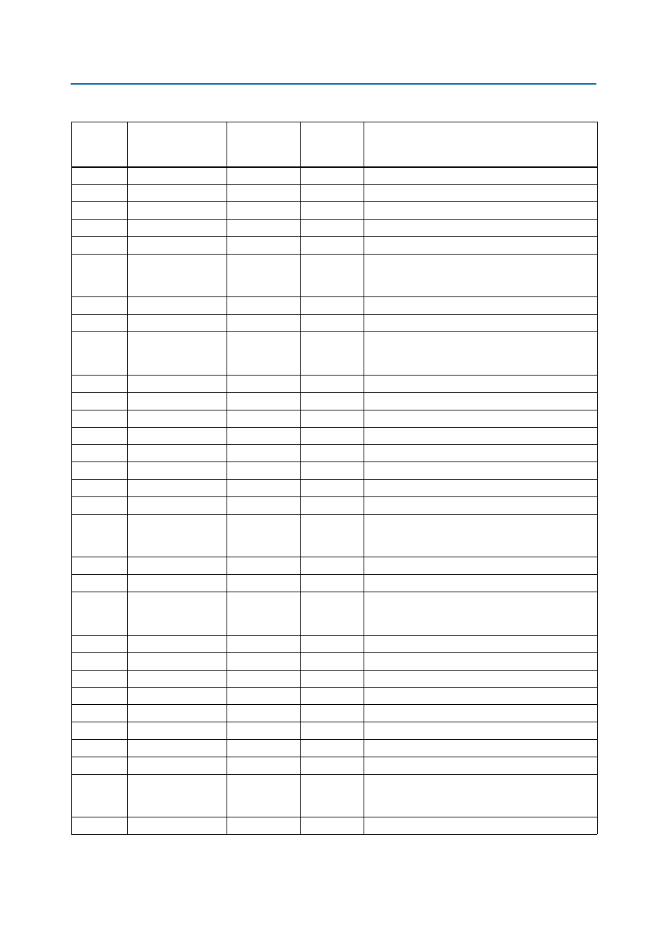
SFP0_TXFAULT
2.5-V LVCMOS
BA9
Interface transmitter fault
48
SFP1_LOS
2.5-V LVCMOS
AG13
Signal loss indicator from the SFP+ interface
46
SFP1_MOD0_PRSNTN
2.5-V LVCMOS
BA33
Module present indicator from the SFP+ interface
45
SFP1_MOD1_SCL
2.5-V LVCMOS
AL20
Two-wire serial interface clock line
44
SFP1_MOD2_SDA
2.5-V LVCMOS
AR33
Two-wire serial interface data line
47
SFP1_RATESEL
2.5-V LVCMOS
AR35
Rate select. Controls the SFP+ interface receiver.
When input signaling is high, the rate is > 4.25 GBps
and when input signaling is low, the rate
≤ 4.25 GBps.
52
SFP1_RDN
1.5-V PCML
P1
Received data (output from the SFP+ interface)
53
SFP1_RDP
1.5-V PCML
P2
Received data (output from the SFP+ interface)
49
SFP1_RS1
2.5-V LVCMOS
AY12
Rate select. Controls the SFP+ interface transmitter.
When input signaling is high, the rate is > 4.25 GBps
and when input signaling is low, the rate
≤ 4.25 GBps.
59
SFP1_TDN
1.5-V PCML
L3
Transmitted data (input to the SFP+ interface)
58
SFP1_TDP
1.5-V PCML
L4
Transmitted data (input to the SFP+ interface)
43
SFP1_TXDISABLE
2.5-V LVCMOS
AU36
Turns off and disables the transmitter laser output
42
SFP1_TXFAULT
2.5-V LVCMOS
BB21
Interface transmitter fault
28
SFP2_LOS
2.5-V LVCMOS
AF11
Signal loss indicator from the SFP+ interface
26
SFP2_MOD0_PRSNTN
2.5-V LVCMOS
AP21
Module present indicator from the SFP+ interface
25
SFP2_MOD1_SCL
2.5-V LVCMOS
AN33
Two-wire serial interface clock line
24
SFP2_MOD2_SDA
2.5-V LVCMOS
AE30
Two-wire serial interface data line
27
SFP2_RATESEL
2.5-V LVCMOS
BD10
Rate select. Controls the SFP+ interface receiver.
When input signaling is high, the rate is > 4.25 GBps
and when input signaling is low, the rate
≤ 4.25 GBps.
32
SFP2_RDN
1.5-V PCML
B1
Received data (output from the SFP+ interface)
33
SFP2_RDP
1.5-V PCML
B2
Received data (output from the SFP+ interface)
29
SFP2_RS1
2.5-V LVCMOS
BC37
Rate select. Controls the SFP+ interface transmitter.
When input signaling is high, the rate is > 4.25 GBps
and when input signaling is low, the rate
≤ 4.25 GBps.
39
SFP2_TDN
1.5-V PCML
F5
Transmitted data (input to the SFP+ interface)
38
SFP2_TDP
1.5-V PCML
F6
Transmitted data (input to the SFP+ interface)
23
SFP2_TXDISABLE
2.5-V LVCMOS
AN22
Turns off and disables the transmitter laser output
22
SFP2_TXFAULT
2.5-V LVCMOS
AY36
Interface transmitter fault
8
SFP3_LOS
2.5-V LVCMOS
AF10
Signal loss indicator from the SFP+ interface
6
SFP3_MOD0_PRSNTN
2.5-V LVCMOS
AD32
Module present indicator from the SFP+ interface
5
SFP3_MOD1_SCL
2.5-V LVCMOS
BB12
Two-wire serial interface clock line
4
SFP3_MOD2_SDA
2.5-V LVCMOS
AM11
Two-wire serial interface data line
7
SFP3_RATESEL
2.5-V LVCMOS
AE31
Rate select. Controls the SFP+ interface receiver.
When input signaling is high, the rate is > 4.25 GBps
and when input signaling is low, the rate
≤ 4.25 GBps.
12
SFP3_RDN
1.5-V PCML
C3
Received data (output from the SFP+ interface)
Table 2–29. SFP+ Interface Pin Assignments, Schematic Signal Names, and Functions (Part 2 of 3)
Board
Reference
(J10)
Schematic Signal
Name
I/O Standard
Stratix V GX
Device Pin
Number
Description