Altera 100G Development Kit, Stratix V GX Edition User Manual
Page 33
Chapter 2: Board Components
2–25
Clock Circuitry
August 2012
Altera Corporation
100G Development Kit, Stratix V GX Edition
Reference Manual
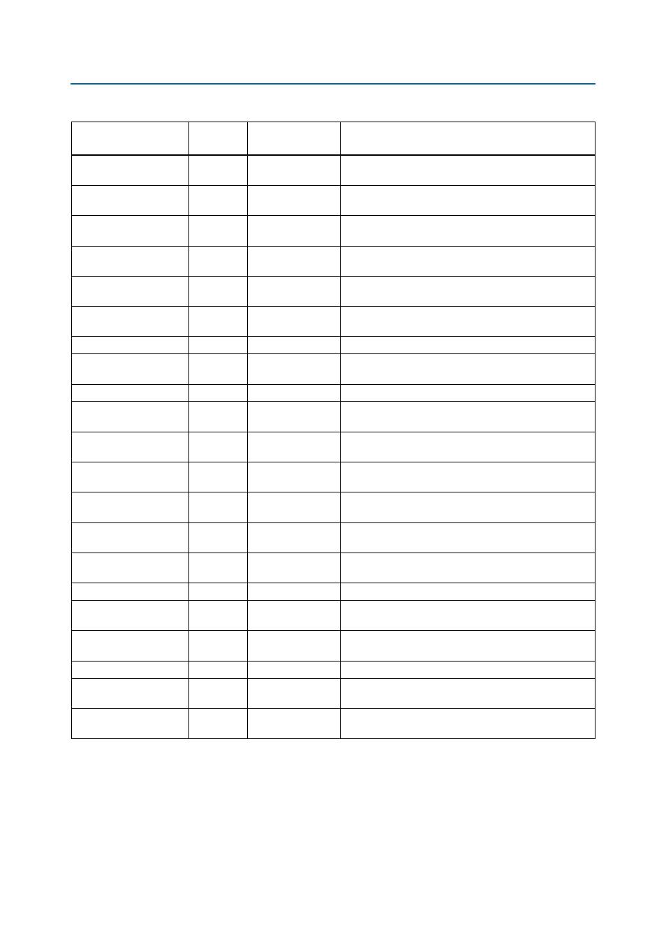
REFCLK_QR0_N/P
LVDS
AK39/AK38
Differential programmable clock to reference clock for the
transceivers that go to the Interlaken interface.
REFCLK_QR1_N/P
LVDS
AF39/AF38
Differential programmable clock to reference clock for the
transceivers that go to the Interlaken interface.
REFCLK_QR2_N/P
LVDS
AB40/AB39
Differential programmable clock to reference clock for the
transceivers that go to the Interlaken interface.
REFCLK_QR3_N/P
LVDS
V40/V39
Differential programmable clock to reference clock for the
transceivers that go to the Interlaken interface.
QDR2A_CLK_IN_N/P
LVDS
BB27/BA27
Differential programmable clock to the FPGA fabric for the
QDRII interface.
QDR2B_CLK_IN_N/P
LVDS
BD8/BC8
Differential programmable clock to the FPGA fabric for the
QDRII interface.
VCXOB_CLK_IN_N/P
LVDS
BC34/BB33
Differential programmable clock to I/O bank 3B for 1588.
DDR3A_CLK_IN_N/P
LVDS
F16/G16
Differential programmable clock to the FPGA fabric for the
DDR3 interface.
SMA_DIFF_CLKIN_N/P0
LVDS
—
SMA input to FPGA reference clocks for the FPGA fabric.
REFCLK_OSC_N/P
LVDS
—
SMA input to FPGA reference clocks for transceivers to
optical interfaces.
SMA_REF_CLKIN_N/P
LVDS
—
SMA input to FPGA reference clocks for transceivers to
Interlaken interface.
SMA_DIFF_CLKIN_N/P1
LVDS
—
SMA input to FPGA reference clocks for transceivers to
Interlaken interface.
BUFFB_CLK_N/P
LVDS
—
SMA buffered output of reference clocks distribute to
transceivers for Interlaken interface.
REFCLK_QL_N/P
LVDS
—
SMA buffered output of reference clocks distributed to
transceivers for optical interfaces.
OPTIC_CLK_N/P
LVDS
—
SMA buffered output of divide-by-four clock distributed to
the CFP optical interface.
BUFFA_DIFF_CLK_N/P
LVDS
—
SMA buffered output to clocks distributed to FPGA fabric.
BUFFA_REF_CLK0_N/P
LVDS
—
SMA buffered output of reference clocks distribute to
transceivers for Interlaken interface.
BUFFA_REF_CLK1_N/P
LVDS
—
SMA buffered output of reference clocks distribute to
transceivers for Interlaken interface.
CLK_644_N/P
LVDS
—
644.53125 MHz SMA output clock.
CLK_CONFIG
2.5-V
LVCMOS
—
100 MHz clock that goes to the MAX II System Controller
for the PFL.
CLKIN_50_FPGA
2.5-V
LVCMOS
AY9
50 MHz clock that goes to the Stratix V GX and MAX II
System Controller.
Table 2–14. Clock Circuitry Pin-Out (Part 2 of 2)
Schematic
Signal Name
I/O
Standard
Stratix V GX Device
Pin Name
Description