Altera 100G Development Kit, Stratix V GX Edition User Manual
Page 20
2–12
Chapter 2: Board Components
MAX II CPLD EPM2210 System Controller
100G Development Kit, Stratix V GX Edition
August 2012
Altera Corporation
Reference Manual
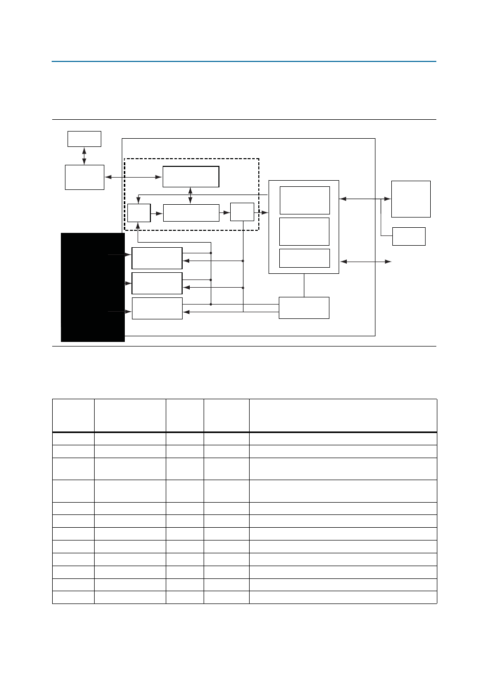
illustrates the MAX II CPLD EPM2210 System Controller's functionality
and external circuit connections.
lists the I/O signals present on the MAX
II CPLD EPM2210 System
Controller. The signal names and functions are relative to the MAX
II device (U59).
Figure 2–2. MAX II CPLD EPM2210 System Controller Block Diagram
LM95235
Controller
Information
Register
On-Board
USB-Blaster II
MAX II CPLD
Si5338
Controller
SLD-HUB
PFL
FSM BUS
Virtual-JTAG
PC
FPGA
LTC2418
Controller
FLASH
Decoder
Encoder
GPIO
JTAG Control
Control
Register
Fast Configuration
Downloader
Table 2–5. MAX II CPLD EPM2210 System Controller Device Pin-Out (Part 1 of 5)
Board
Reference
(U59)
Schematic Signal
Name
I/O
Standard
Stratix V GX
Device Pin
Number
Pin Description
R18
CLK125_EN
2.5-V
—
125-MHz oscillator clock enable
D16
CLK50_EN
2.5-V
—
50-MHz oscillator clock enable
D2
CLK_1588_SEL
2.5-V
—
Programmable VCXO enable signal for the clock to FPGA
bank 3B
C2
CLK_SFP_SEL
2.5-V
—
Programmable VCXO enable signal for the clock to FPGA
bank QR1
J6
CLKIN_50_MAX
2.5-V
—
50-MHz oscillator clock enable
H17
CONFIGN_LED
2.5-V
—
FPGA initialization LED
J1
CSENSE_SCK
2.5-V
—
Power monitor SPI clock
H6
CSENSE_SDI
2.5-V
—
Power monitor SPI input data
K1
CSENSE_SDO
2.5-V
—
Power monitor SPI output data
R12
EXTRA_SIG0
1.5-V
—
Extra signal
V14
EXTRA_SIG1
1.5-V
—
Extra signal
P12
EXTRA_SIG2
1.5-V
—
Extra signal