Development board block diagram, Handling the board – Altera 100G Development Kit, Stratix V GX Edition User Manual
Page 7
Chapter 1: Overview
1–3
Development Board Block Diagram
August 2012
Altera Corporation
100G Development Kit, Stratix V GX Edition
Reference Manual
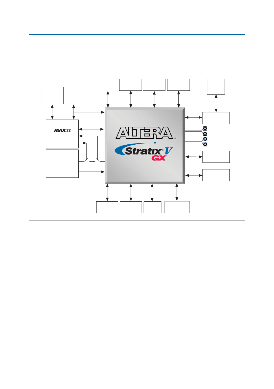
Development Board Block Diagram
shows the block diagram of the Stratix V GX 100G development board.
Handling the Board
When handling the board, it is important to observe the following static discharge
precaution:
c
Without proper anti-static handling, the board can be damaged. Therefore, use
anti-static handling precautions when touching the board.
The Stratix V GX 100G development board must be stored between –40º C and 100º C.
The recommended operating temperature is between 0º C and 55º C.
Figure 1–1. Stratix V GX 100G Development Board Block Diagram
5SGXEA7N2F45C2
CPLD
(x32)
User LEDs,
Push Buttons
User LEDs,
Push Buttons
On-Board
USB-Blaster
10/100/1000
Ethernet
RJ45
Jack
4 MB QDR II
(x18)
4 MB QDR II
(x36)
64 MB
Flash
CFP
QSFP
QSFP
Clocks
& PLL
6 DDR3 SDRAM
(x32)
Interlaken
Transceivers
Connected to
SMA Connectors
4 SFP+
Modules