Altera 100G Development Kit, Stratix V GX Edition User Manual
Page 32
2–24
Chapter 2: Board Components
Clock Circuitry
100G Development Kit, Stratix V GX Edition
August 2012
Altera Corporation
Reference Manual
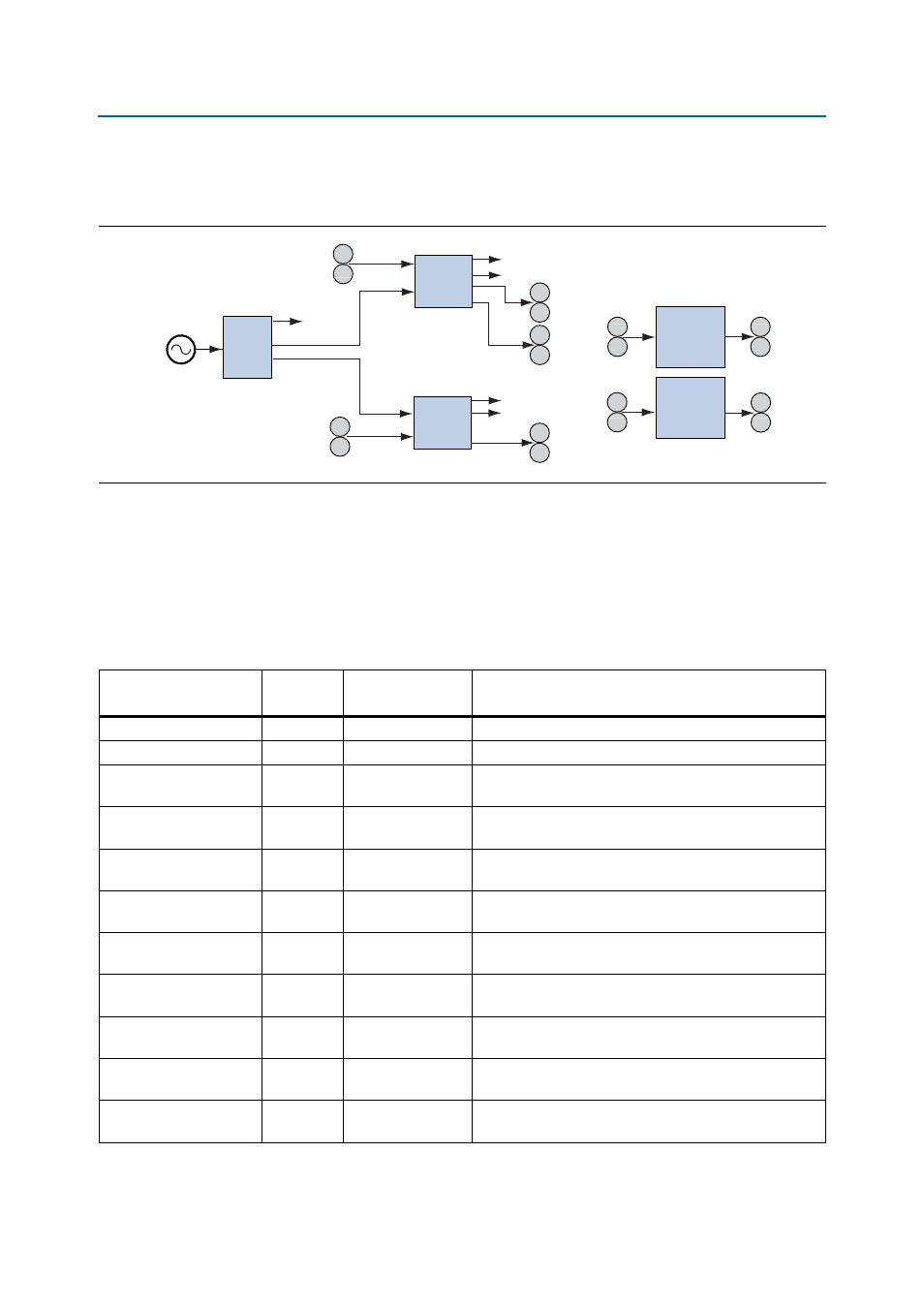
shows the Stratix V GX development board clock tree structure for the
Interlaken side and DDR3 interface.
You can select between the PLL or an off-board clock for the clock distribution path by
using the board settings DIP switch (SW3). This DIP switch is located near the bottom
left corner of the board. Refer to
for the switch settings and
descriptions. The DIP switch with USB_DISABLEn label connects to the MAX II device
and controls the traffic that passes through the USB connector.
lists the clock signal names, I/O standards, and functional descriptions.
Figure 2–7. Stratix V GX Development Board Clock Tree Structure for Interlaken Side and DDR3 Interface
LVDS
Clock Buffer
MUX
LVDS
Clock Buffer
MUX
PLL
Interlaken
x12
Interlaken
x12
25 MHz
625 MHz
SMA
SMA
SMA
SMA
SMA
SMA
SMA
SMA
SMA
SMA
SMA
SMA
SMA
SMA
SMA
SMA
SMA
SMA
625 MHz
REFCLK_QR1
REFCLK_QR2
REFCLK_QR0
REFCLK_QR3
DDR3_CLK
100 MHz
Si5338
ICS8543
ICS8543
Table 2–14. Clock Circuitry Pin-Out (Part 1 of 2)
Schematic
Signal Name
I/O
Standard
Stratix V GX Device
Pin Name
Description
DIFFCLK_IN1_N/P
LVDS
BA34/AY34
Differential programmable clock to I/O bank 3B.
CLKIN_125_N/P
LVDS
BA18/AY18
Differential fixed clock to I/O bank 3B for Ethernet.
REFCLK_QL0_N/P
LVDS
AK6/AK7
Differential programmable clock to reference clock for the
transceivers that go to the optical interfaces.
REFCLKB_QL0_N/P
LVDS
AH5/AH6
Differential programmable clock to reference clock for the
transceivers that go to the optical interfaces.
REFCLK_QL1_N/P
LVDS
AF6/AF7
Differential programmable clock to reference clock for the
transceivers that go to the optical interfaces.
REFCLK_QL2_N/P
LVDS
AB5/AB6
Differential programmable clock to reference clock for the
transceivers that go to the optical interfaces.
REFCLKB_QL2_N/P
LVDS
Y6/Y7
Differential programmable clock to reference clock for the
transceivers that go to the optical interfaces.
REFCLK_QL3_N/P
LVDS
V5/V6
Differential programmable clock to reference clock for the
transceivers that go to the optical interfaces.
SMA_REFCLK_N/P
LVDS
T6/T7
Reference clock SMA input to transceivers that go to the
optical interfaces.
PRGCLK_QL1_N/P
LVDS
AD5/AD6
Differential programmable clock to reference clock for the
transceivers that go to the optical interfaces.
CFP_REFCLK_N/P
CML
—
Divide-by-four differential programmable clock to the
reference clock for the CFP interface.