External memory interfaces, Ddr3 interface, External memory interfaces –44 – Altera 100G Development Kit, Stratix V GX Edition User Manual
Page 52: Ddr3 interface –44
2–44
Chapter 2: Board Components
Components and Interfaces
100G Development Kit, Stratix V GX Edition
August 2012
Altera Corporation
Reference Manual
lists the Interlaken interface component reference and manufacturing
information.
External Memory Interfaces
This section describes the development board’s memory interface support, signal
names, types, and connectivity relative to the Stratix V GX device.
The development board contains two types of external memory interfaces that utilizes
the top and bottom of the Stratix V GX device.
■
DDR3 Interface—3 GB of high-speed DRAM for packet storage and other
sequential access memory uses.
■
QDR II Interface—9 MB of quad-port SRAM for high-speed random access
applications such as lookup tables and packet inspection.
f
For more information about the memory interfaces, refer to the
DDR3 Interface
The DDR3 interface consists of 12 DDR3 devices, each providing 256-MB with a 16-bit
data bus. The maximum target speed is 800 MHz DDR for a theoretical bandwidth of
over 51.2 Gbps per 32-bit port, or a total bandwidth of 307.2 Gbps for the full 192-bit
bus. The targeted Micron device is rated at 800 MHz with a CAS latency of 11.
1
The board will be adapted to support the 933 MHz devices from Micron as a drop in
replacement once they become available.
G3
INT_RX_P21
1.5-V PCML
T43
Receive XCVR pair 21 to FPGA
H3
INT_RX_N21
1.5-V PCML
T44
Receive XCVR pair 21 to FPGA
J4
INT_RX_P22
1.5-V PCML
H43
Receive XCVR pair 22 to FPGA
K4
INT_RX_N22
1.5-V PCML
H44
Receive XCVR pair 22 to FPGA
G1
INT_RX_P23
1.5-V PCML
Y43
Receive XCVR pair 23 to FPGA
H1
INT_RX_N23
1.5-V PCML
Y44
Receive XCVR pair 23 to FPGA
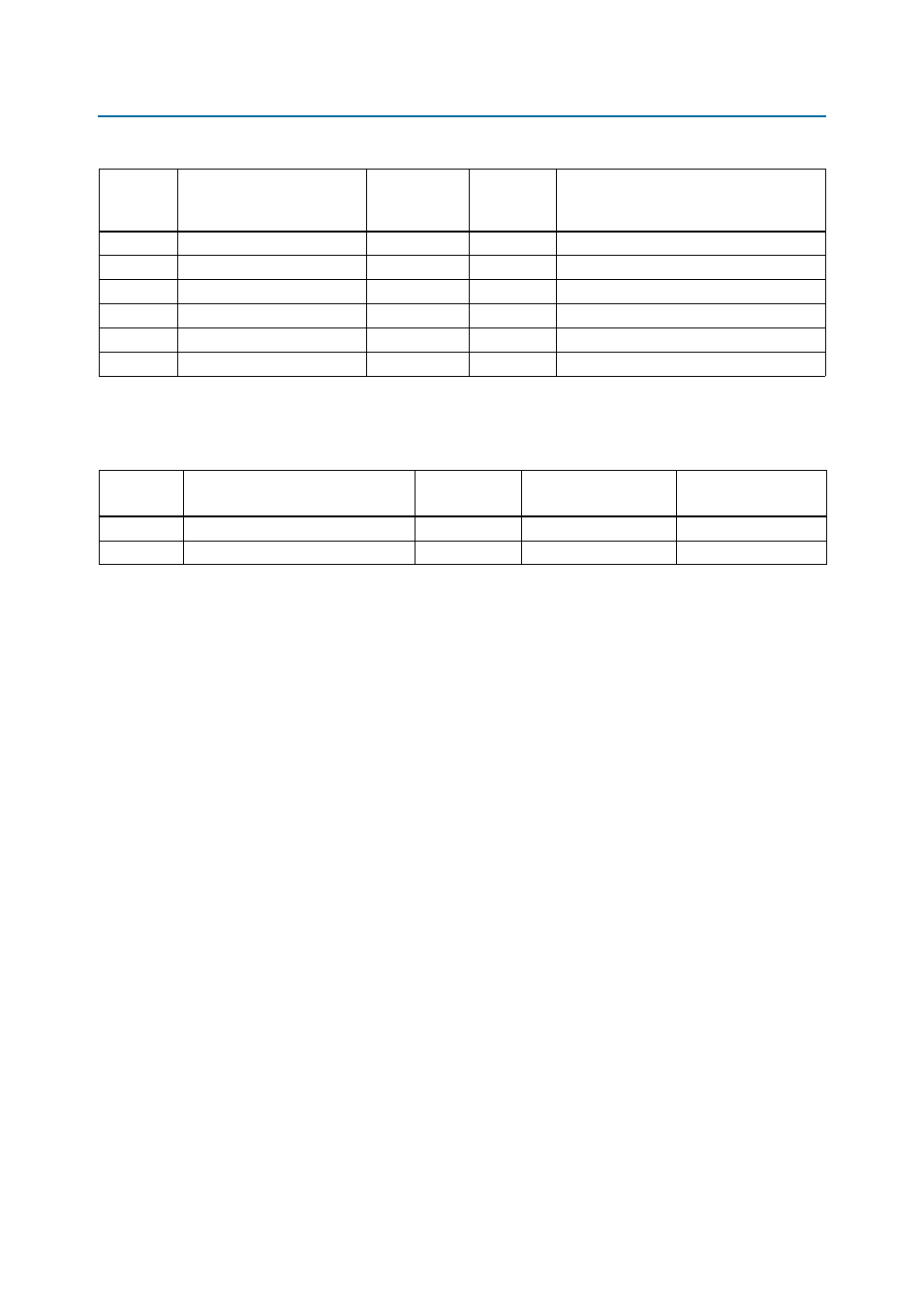
Table 2–33. Interlaken Interface Pin Assignments, Schematic Signal Names, and Functions (Part 5 of 5)
Board
Reference
Schematic Signal Name
I/O Standard
Stratix V GX
Device Pin
Number
Description
Table 2–34. Interlaken interface Component Reference And Manufacturing Information
Board
Reference
Description
Manufacturer
Manufacturing
Part Number
Manufacturer
Website
J16, J60
Interlaken interface header
FCI
10035515-101LF
J4, J38
Interlaken interface receptical
FCI
10045722-101LF