Clock circuitry, Clock circuitry –23 – Altera 100G Development Kit, Stratix V GX Edition User Manual
Page 31
Chapter 2: Board Components
2–23
Clock Circuitry
August 2012
Altera Corporation
100G Development Kit, Stratix V GX Edition
Reference Manual
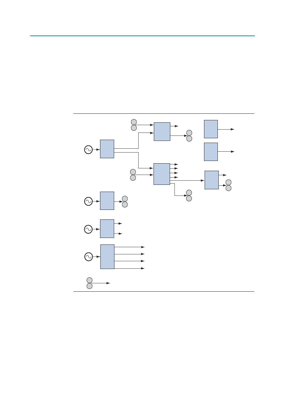
Clock Circuitry
The clock tree structure for the line side and QDRII interface on the Stratix V GX
board is made up of two programmable quad PLLs where each output can be
programmed for a specific frequency. The default frequency for the clocks going to
QL0 through QL3 is 644.53125 MHz and the default frequency going to the QDRII
interface is 100 MHz.
shows the Stratix V GX development board clock tree structure for the line
side and QDRII interface.
The clock tree structure for the Interlaken interface and the DDR3 interface uses one
programmable on-board quad PLL to generate the necessary frequencies. The default
frequency for the Interlaken interface is 625 MHz and for the DDR3 interface is
100 MHz.
Figure 2–6. Development Board Clock Tree Structure for Line Side and QDRII Interface
LVDS
Clock Buffer
MUX
LVDS
Clock Buffer
MUX
PLL
25 MHz
SMA
SMA
SMA
SMA
SMA
SMA
SMA
SMA
SMA
SMA
SMA
SMA
SMA
125 MHz
644.53125 MHz
644.53125 MHz
644.53125 MHz
644.53125 MHz
644.53125 MHz
REFCLK_QR1
REFCLK_QR2
REFCLK_QR3
REFCLK_QR3
REFCLK_QR0
REFCLK_QR0
REFCLK_QR2
QDRII_CLK
QDRII_CLK
50MHZ_STRATIX
50MHZ_MAX_II
REFCLK_QR3
CFP
PLL
1588
PLL
REFCLK_QL1
Optical Clock
100 MHz
100 MHz
100 MHz
Si5338
NB6L11SMNG
50 MHz
PLL
25 MHz
Si5338
Si571
Si571
MC100ES6139
Divide-by-4
Differential
Clock
ICS8543
ICS8543
LVDS
Clock
Buffer
Clock
Buffer
SMA