Altera 100G Development Kit, Stratix V GX Edition User Manual
Page 51
Chapter 2: Board Components
2–43
Components and Interfaces
August 2012
Altera Corporation
100G Development Kit, Stratix V GX Edition
Reference Manual
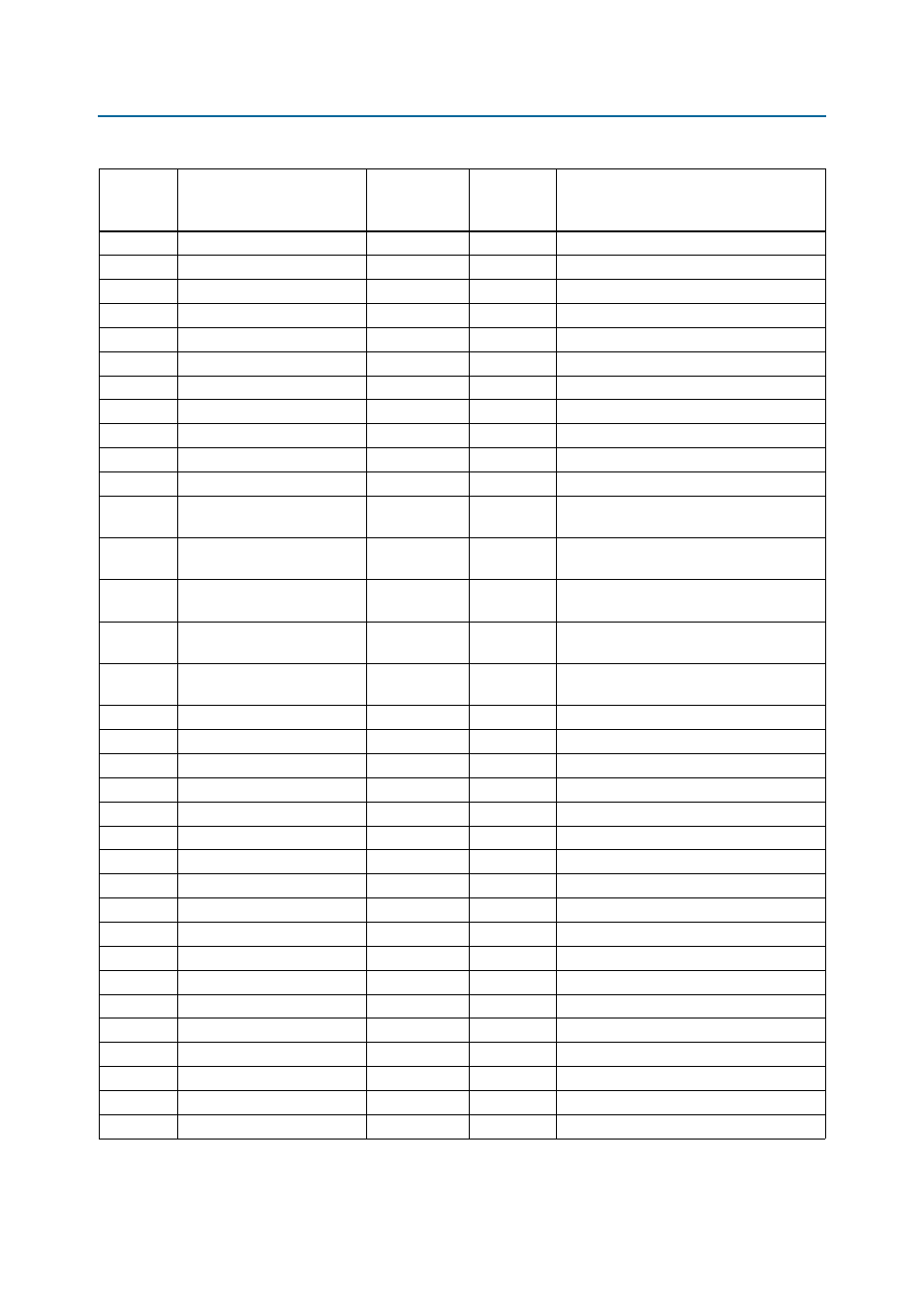
E4
INT_TX_N18
1.5-V PCML
L42
Transmit XCVR pair 18 from FPGA
A5
INT_TX_P19
1.5-V PCML
K39
Transmit XCVR pair 19 from FPGA
B5
INT_TX_N19
1.5-V PCML
K40
Transmit XCVR pair 19 from FPGA
G5
INT_TX_P20
1.5-V PCML
J41
Transmit XCVR pair 20 from FPGA
H5
INT_TX_N20
1.5-V PCML
J42
Transmit XCVR pair 20 from FPGA
G3
INT_TX_P21
1.5-V PCML
N41
Transmit XCVR pair 21 from FPGA
H3
INT_TX_N21
1.5-V PCML
N42
Transmit XCVR pair 21 from FPGA
J4
INT_TX_P22
1.5-V PCML
H39
Transmit XCVR pair 22 from FPGA
K4
INT_TX_N22
1.5-V PCML
H40
Transmit XCVR pair 22 from FPGA
G1
INT_TX_P23
1.5-V PCML
U41
Transmit XCVR pair 23 from FPGA
H1
INT_TX_N23
1.5-V PCML
U42
Transmit XCVR pair 23 from FPGA
B1
INT_MSB_CON_RX_CLK_N
LVDS
—
Receive clock for the second 12 bits of the
bus
A1
INT_MSB_CON_RX_CLK_P
LVDS
—
Receive clock for the second 12 bits of the
bus
E10
INT_MSB_CON_RX_FC_CK
2.5-V LVCMOS
AJ20
Receive flow control clock signal for the
second 12 bits of the bus
H7
INT_MSB_CON_RX_FC_DATA
2.5-V LVCMOS
AL35
Receive flow control data signal for the
second 12 bits of the bus
H9
INT_MSB_CON_RX_FC_SYNC
2.5-V LVCMOS
BD11
Receive flow control synchronization signal
for the second 12 bits of the bus
A7
INT_RX_P12
1.5-V PCML
B43
Receive XCVR pair 12 to FPGA
B7
INT_RX_N12
1.5-V PCML
B44
Receive XCVR pair 12 to FPGA
D6
INT_RX_P13
1.5-V PCML
F43
Receive XCVR pair 13 to FPGA
E6
INT_RX_N13
1.5-V PCML
F44
Receive XCVR pair 13 to FPGA
D8
INT_RX_P14
1.5-V PCML
D43
Receive XCVR pair 14 to FPGA
E8
INT_RX_N14
1.5-V PCML
D44
Receive XCVR pair 14 to FPGA
A9
INT_RX_P15
1.5-V PCML
C43
Receive XCVR pair 15 to FPGA
B9
INT_RX_N15
1.5-V PCML
C44
Receive XCVR pair 15 to FPGA
A3
INT_RX_P16
1.5-V PCML
V43
Receive XCVR pair 16 to FPGA
B3
INT_RX_N16
1.5-V PCML
V44
Receive XCVR pair 16 to FPGA
D2
INT_RX_P17
1.5-V PCML
AB43
Receive XCVR pair 17 to FPGA
E2
INT_RX_N17
1.5-V PCML
AB44
Receive XCVR pair 17 to FPGA
D4
INT_RX_P18
1.5-V PCML
P43
Receive XCVR pair 18 to FPGA
E4
INT_RX_N18
1.5-V PCML
P44
Receive XCVR pair 18 to FPGA
A5
INT_RX_P19
1.5-V PCML
K43
Receive XCVR pair 19 to FPGA
B5
INT_RX_N19
1.5-V PCML
K44
Receive XCVR pair 19 to FPGA
G5
INT_RX_P20
1.5-V PCML
M43
Receive XCVR pair 20 to FPGA
H5
INT_RX_N20
1.5-V PCML
M44
Receive XCVR pair 20 to FPGA
Table 2–33. Interlaken Interface Pin Assignments, Schematic Signal Names, and Functions (Part 4 of 5)
Board
Reference
Schematic Signal Name
I/O Standard
Stratix V GX
Device Pin
Number
Description