Sfp+ interface, Sfp+ interface –35 – Altera 100G Development Kit, Stratix V GX Edition User Manual
Page 43
Chapter 2: Board Components
2–35
Components and Interfaces
August 2012
Altera Corporation
100G Development Kit, Stratix V GX Edition
Reference Manual
lists the QSFP interfaces component reference and manufacturing
information.
SFP+ Interface
The development board consists of four SFP+ interfaces. All the SPF+ interfaces
connect directly to the Stratix V GX transceivers. The SFP+ interfaces can support
datacom applications such as 8.5 GBd Fibre Channel, 10 Gigabit Ethernet, or
10 Gigabit Fibre Channel.
lists the pin assignments for the SFP+ interface and their corresponding
schematic signal names and Stratix V GX pin numbers.
2
QSFP1_TX_N1
1.5-V PCML
H5
Transmit XCVR pair 1 from FPGA
33
QSFP1_TX_P2
1.5-V PCML
G4
Transmit XCVR pair 2 from FPGA
34
QSFP1_TX_N2
1.5-V PCML
G3
Transmit XCVR pair 2 from FPGA
6
QSFP1_TX_P3
1.5-V PCML
E4
Transmit XCVR pair 3 from FPGA
5
QSFP1_TX_N3
1.5-V PCML
E3
Transmit XCVR pair 3 from FPGA
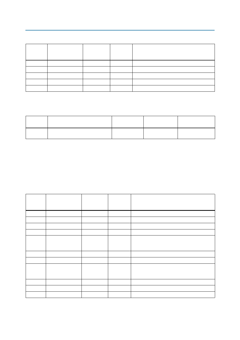
Table 2–27. QSFP Interface Pin Assignments, Schematic Signal Names, and Functions (Part 2 of 2)
Board
Reference
(J19)
Schematic Signal
Name
I/O Standard
Stratix V GX
Device Pin
Number
Description
Table 2–28. QSFP interfaces Component Reference And Manufacturing Information
Board
Reference
Description
Manufacturer
Manufacturing
Part Number
Manufacturer
Website
J33, J19
Single-port, family-standard QSFP cage,
right-angle, press-fit connector
Tyco Electronics
1888617-1
Table 2–29. SFP+ Interface Pin Assignments, Schematic Signal Names, and Functions (Part 1 of 3)
Board
Reference
(J10)
Schematic Signal
Name
I/O Standard
Stratix V GX
Device Pin
Number
Description
68
SFP0_LOS
2.5-V LVCMOS
AY10
Signal loss indicator from the SFP+ interface
66
SFP0_MOD0_PRSNTN
2.5-V LVCMOS
BB9
Module present indicator from the SFP+ interface
65
SFP0_MOD1_SCL
2.5-V LVCMOS
BB35
Two-wire serial interface clock line
64
SFP0_MOD2_SDA
2.5-V LVCMOS
AV34
Two-wire serial interface data line
67
SFP0_RATESEL
2.5-V LVCMOS
AT9
Rate select. Controls the SFP+ interface receiver.
When input signaling is high, the rate is > 4.25 GBps
and when input signaling is low, the rate
≤ 4.25 GBps.
72
SFP0_RDN
1.5-V PCML
AF1
Received data (output from the SFP+ interface)
73
SFP0_RDP
1.5-V PCML
AF2
Received data (output from the SFP+ interface)
69
SFP0_RS1
2.5-V LVCMOS
AP34
Rate select. Controls the SFP+ interface transmitter.
When input signaling is high, the rate is > 4.25 GBps
and when input signaling is low, the rate
≤ 4.25 GBps.
79
SFP0_TDN
1.5-V PCML
AC3
Transmitted data (input to the SFP+ interface)
78
SFP0_TDP
1.5-V PCML
AC4
Transmitted data (input to the SFP+ interface)
63
SFP0_TXDISABLE
2.5-V LVCMOS
AT8
Turns off and disables the transmitter laser output