Altera 100G Development Kit, Stratix V GX Edition User Manual
Page 11
Chapter 2: Board Components
2–3
Board Overview
August 2012
Altera Corporation
100G Development Kit, Stratix V GX Edition
Reference Manual
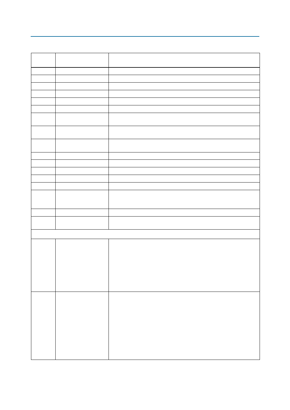
D1
Power LED
Indicates the board power status.
D20-D23
Ethernet status LEDs
Indicates the Ethernet connection speed as well as transmit or receive activity.
D31
Factory POF LED
Illuminates when the factory design is being loaded into the FPGA.
D32
Load LED
Illuminates when the FPGA is being configured.
D24
Error LED
Illuminates when the FPGA configuration from flash fails.
D25
Configuration done LED
Illuminates when the FPGA is successfully configured.
J62
MAX_JTAG_EN jumper
Bypasses the MAX II CPLD EPM2210 System Controller in the JTAG chain when
shunted.
J59
JTAG programming header
JTAG programming header for connecting an Altera USB-Blaster dongle to
program the FPGA and MAX II CPLD devices.
J65
JTAG for on-board
USB-Blaster II
JTAG for on-board USB-Blaster MAX II CPLD device programming.
S1
CPU reset push button
Resets the FPGA logic.
S7
Reset push button
Resets the MAX
II CPLD EPM2210 System Controller logic.
S8
PGM_SEL push button
Selects which design file to load into the FPGA.
S5
Load push button
Initiates loading of the FPGA.
S6
Factory push button
Initiates loading of factory design into the FPGA.
SW3
Board settings DIP switch
Controls the MAX
II CPLD EPM2210 System Controller functions such as clock
enable, power and temperature monitor, as well as voltage settings for
transceivers and SMA clock input control.
U59
MAX II CPLD (System)
Altera EPM2210F324C3N, MAX II CPLD for MAX II+FPP configuration.
U62
MAX II CPLD (On-Board
USB-Blaster II)
Altera EPM570GF100, MAX II CPLD for on-board USB-Blaster II circuitry.
Clock Circuitry
J41, J50
J17, J21
J18, J22
J43, J52
J46, J55
J20, J23
J58, J63
SMA input clocks
LVDS differential clock input to I/O bank 3.
LVDS reference clock input for the optical interfaces
LVDS reference clock input for Stratix V GX device for the optical interfaces.
Center LVDS reference clock inputs for the Interlaken interface.
Outer LVDS reference clock inputs for the Interlaken interface.
LVDS reference clock input for upper 12 bits of the Interlaken interface.
LVDS reference clock input for lower 12 bits of the Interlaken interface.
J42, J51
J11, J14
J12, J15
J8, J13
J44, J53
J45, J54
J47, J56
J5, J6
J27, J28
SMA output clocks
Differential SMA clock output for I/O bank 3.
Reference SMA clock output for the optical interfaces.
SMA output clock divided for the CFP interface.
644.53125 MHz LVDS clock.
LVDS SMA output clock for the Interlaken interface.
LVDS SMA output clock for the Interlaken interface.
LVDS SMA output clock for the Interlaken interface.
SMA output clock from upper 12 bits of the Interlaken interface.
SMA output clock from lower 12 bits of the Interlaken interface.
Table 2–1. Stratix V GX 100G Development Board Components (Part 2 of 4)
Board
Reference
Type
Description