Replacing dsd drive control pcb – Yaskawa DSD 406 User Manual
Page 83
4
Maintenance
79
Replacing DSD Drive Control PCB
3/21/96
Replacing DSD
Drive Control
PCB
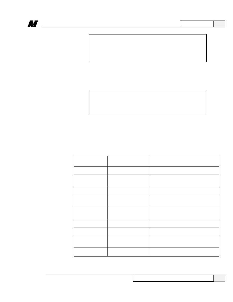
* Either connector J1 or J2 will be present on the board.
Connector
Type
Function
Table 4. Connectors on Drive Control PCB
* RS422 Communications Port.
* RS 232 Port for Portable Control/
Display Unit (PCDU).
Optional LAN Connection.
Power Supply, E-Stop, Motor Thermal
Guard, Loop Contactor Control.
Connector for auxiliary Interface
Card (optional).
Field Control.
Armature Firing Control.
Analog and Digital Local I/O.
Earth Ground
J1
J2
J3
J11
J12
J13
J14
TB1
TB11
DB-9
RJ12 Connector
BNC Connector
20 Pin Header
40 Pin Header
10 Pin Header
40 Pin Header
Screw Terminals
(12 Gauge Wire)
Bare Screw Terminal
CAUTION
The DSD Drive Control PCB has electrostatic sensitive
components. You must follow Electrostatic Discharge (ESD)
procedures to protect the components.
To replace the DSD Drive Control PCB, follow this procedure:
NOTE:
You may need a helper to hold the PCB during replacement.
WARNING
Before performing any maintenance, disconnect all input
and output power from the DSD drive.
❏ Remove all input and output power to the DSD drive.
❏ Note where all cables/wires are connected, especially those connected to
TB1 (see Figure 11). Label any cables/wires, as necessary, to insure proper
reinstallation.