Board overview, Board overview –2, Figure 2–1 – Altera 100G Development Kit, Stratix IV GT Edition User Manual
Page 10: Table 2–1
2–2
Chapter 2: Board Components
Board Overview
100G Development Kit, Stratix IV GT Edition Reference Manual
September 2010
Altera Corporation
Board Overview
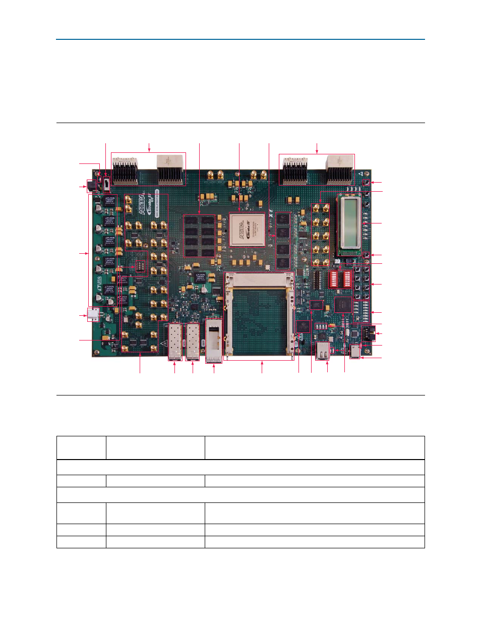
This section provides an overview of the Stratix IV GT 100G development board,
including an annotated board image and component descriptions.
provides an overview of the board features.
describes the components and lists their corresponding board references.
Figure 2–1. Overview of the Stratix IV GT 100G Development Board Features
Power Switch (SW1)
DC Power
Jack (J1)
Power LED
(D7)
LCD Display (J59)
Power
Regulators
MAX II CPLD (U72)
Flash
Memory
(U65)
Board
Settings
DIP Switch
(SW2)
Clock Circuitry
DDR3 Memory
(U28-U31, U36-U39)
User DIP Switches
(SW3, SW4)
Interlaken Channel 0-9 (J39, J57)
Embedded
USB-Blaster
Activity LED (D27)
Ethernet
Status LEDs
(D12-D17)
Embedded
USB-Blaster (J60)
Stratix IV GT FPGA
(U44)
Ethernet
RJ45 Jack
(J49)
User Push-Buttons
(S5-S8)
User LEDs (D28-D35)
JTAG Connector (J61)
SSRAM
(U57)
Interlaken Channel 10-19 (J5, J30)
QDR II Memory
(U47-U50)
Clock Circuitry
Auxiliary
Power
Jack (J2)
SFP Port
B (J31)
SFP Port
A (J32)
QSFP
(J34)
CFP
(J37)
CPU Reset Push-Buttons
(S9)
Factory Push-Buttons
(S12)
Table 2–1. Stratix IV GT 100G Development Board Components (Part 1 of 5)
Board
Reference
Type
Description
Featured Devices
U44
FPGA
EP4S100G5F45I1 Stratix IV GT device in a 1932-Pin FBGA package.
Configuration, Status, and Setup Elements
D25, D20,
D19, D26
Configuration status LEDs
LEDs to indicate the status of FPP configuration.
D7
Power LED
Blue LED to indicate the board power status.
D27
USB-Blaster LED
Green LED to indicate the embedded USB-Blaster activity status.