Qsfp interface, Qsfp interface –39 – Altera 100G Development Kit, Stratix IV GT Edition User Manual
Page 47
Chapter 2: Board Components
2–39
Components and Interfaces
September 2010
Altera Corporation
100G Development Kit, Stratix IV GT Edition Reference Manual
QSFP Interface
The QSFP Interface consists of four full-duplex transceiver channels.
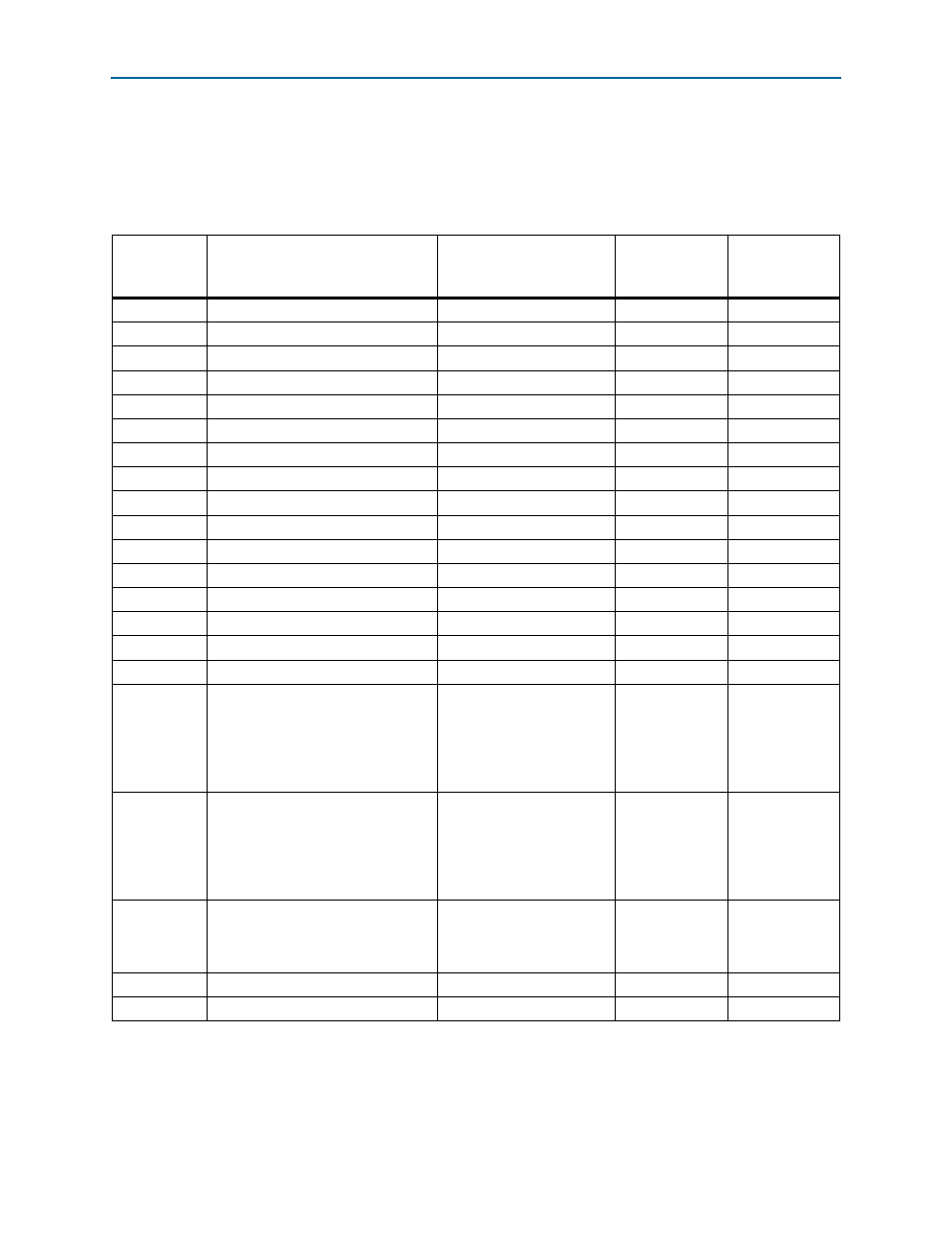
Table 2–29
lists
the pin assignments for the QSFP interface and their corresponding schematic signal
names and Stratix IV GT pin numbers.
Table 2–29. QSFP Interface Pin Assignments, Schematic Signal Names, and Functions
Board
Reference
Description
Schematic
Signal Name
Stratix IV GT
Device
Pin Name
Other
Connections
J34.36
Transmit XCVR pair 0 from FPGA
QSFP_TX_P0
U44.BA7
—
J34.37
Transmit XCVR pair 0 from FPGA
QSFP_TX_N0
U44.BB7
—
J34.3
Transmit XCVR pair 1 from FPGA
QSFP_TX_P1
U44.BA5
—
J34.2
Transmit XCVR pair 1 from FPGA
QSFP_TX_N1
U44.BB5
—
J34.33
Transmit XCVR pair 2 from FPGA
QSFP_TX_P2
U44.AU4
—
J34.34
Transmit XCVR pair 2 from FPGA
QSFP_TX_N2
U44.AU3
—
J34.6
Transmit XCVR pair 3 from FPGA
QSFP_TX_P3
U44.AR4
—
J34.5
Transmit XCVR pair 3 from FPGA
QSFP_TX_N3
U44.AR3
—
J34.17
Receive XCVR pair 0 from FPGA
QSFP_RX_P0
U44.BC8
—
J34.18
Receive XCVR pair 0 from FPGA
QSFP_RX_N0
U44.BD8
—
J34.22
Receive XCVR pair 1 from FPGA
QSFP_RX_P1
U44.BC6
—
J34.21
Receive XCVR pair 1 from FPGA
QSFP_RX_N1
U44.BD6
—
J34.14
Receive XCVR pair 2 from FPGA
QSFP_RX_P2
U44.AV2
—
J34.15
Receive XCVR pair 2 from FPGA
QSFP_RX_N2
U44.AV1
—
J34.25
Receive XCVR pair 3 from FPGA
QSFP_RX_P3
U44.AT2
—
J34.24
Receive XCVR pair 3 from FPGA
QSFP_RX_N3
U44.AT1
—
J34.8
Module select input:
0: Select module for 2-wire serial
communication
1: Module not available for 2-wire
serial communication
QSFP_MOD_SELN
U44.AA38
—
J34.31
Low power mode input:
0: Set module for high-power mode
1: Set module for low-power mode
(maximum power consumption is
1.5 W)
QSFP_LP_MODE
U44.Y39
—
J34.9
Module reset input:
0: Reset module
1: Normal mode
QSFP_RSTN
U44.Y38
—
J34.11
2-wire serial clock input
QSFP_SCL
U44.AB39
—
J34.12
2-wire serial data
QSFP_SDA
U44.AA39
—