Clock circuitry, Clock circuitry –24 – Altera 100G Development Kit, Stratix IV GT Edition User Manual
Page 32
2–24
Chapter 2: Board Components
Clock Circuitry
100G Development Kit, Stratix IV GT Edition Reference Manual
September 2010
Altera Corporation
Clock Circuitry
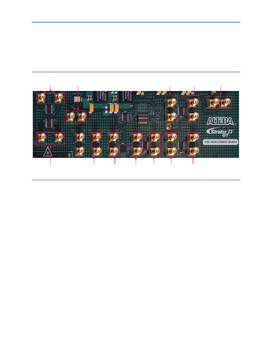
This section describes the clock tree structure for the Stratix IV GT 100G Development
board.
Figure 2–7
shows the Stratix IV GT 100G development board clock circuitry.
The clock tree structure for the board is distributed into two—clock A and clock B.
Clock A is for the Interlaken interface and clock B is for the line side interface. The
PLL/buffer device (Si5338) sources both clock trees which is then distributed to the
reference clock buffer (REF_CLK ) and to the differential clock buffer (DIFF_CLK). The
DIFF_CLK
buffer fans out the clock to dedicated clock inputs on the vertical I/Os of the
FPGA. A third differential clock from the DIFF_CLK buffer goes to the single-ended
clock buffer (SE_CLK). The SE_CLK buffer distributes the clock to every side of the
FPGA.
The REF_CLK for clock A tree structure distributes its input clock to transceiver block 1
and 2 on the right side of the FPGA (or left side of the die). The REF_CLK for clock B
tree structure distributes the clock to all four transceiver blocks on the left side of the
FPGA (or right side of the die).
Figure 2–7. Stratix IV GT 100G Development Board Clock Circuitry
Optical Clock B Out
(For Divide-by-4 Circuit)
Reference Clock A Out
(For Interlaken Side)
Reference Clock A In
(For Interlaken Side)
Buffered Differential
Clock A Out
Differential
Clock A In
Buffered Differential
Clock B Out
Differential
Clock B In
Reference Clock B
In (For Line Side)
Reference Clock B
Out (For Line Side)
644-MHz Clock Out
Single-Ended Clock In/Out B
Single-Ended Clock In/Out A