I/o resources, I/o resources –7 – Altera 100G Development Kit, Stratix IV GT Edition User Manual
Page 15
Chapter 2: Board Components
2–7
Featured Device: Stratix IV GT Device
September 2010
Altera Corporation
100G Development Kit, Stratix IV GT Edition Reference Manual
I/O Resources
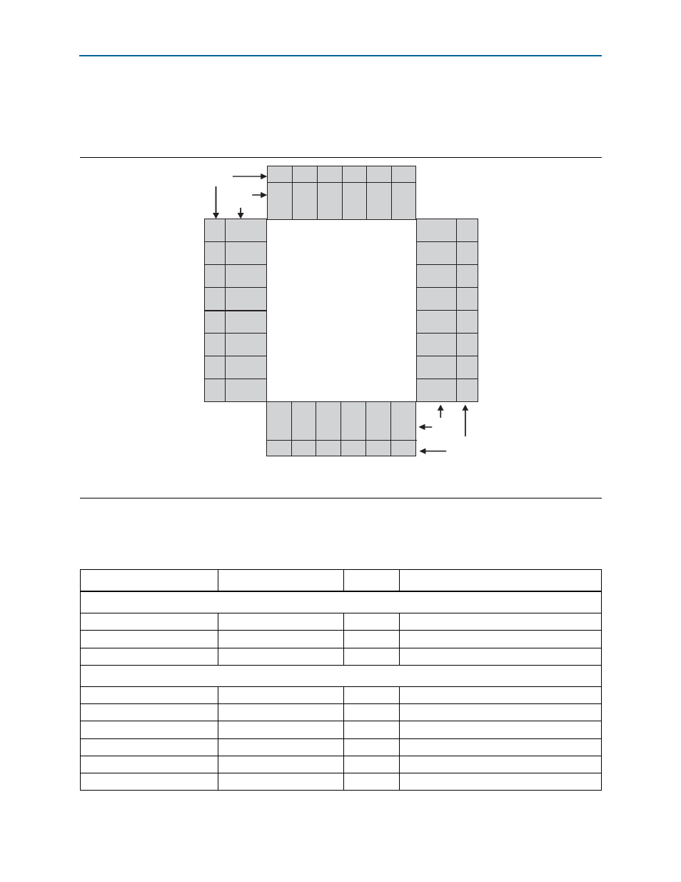
Figure 2–2
shows the bank organization and I/O count for the EP4S100G5F45I1
device in the 1932-pin FBGA package.
summarizes the FPGA I/O usage by function on the Stratix IV GT 100G
development board. I/O direction is with respect to the FPGA.
Figure 2–2. Stratix IV GT Device I/O Bank Diagram
Note to
Figure 2–2
:
(1) There are two additional PMA-only transceiver channels in each transceiver bank.
Ba
nk
8
B
4
8
Ba
nk
7
A
4
8
Ba
nk
7
B
4
8
B
ank
7C
32
21 Bank 1C
21 Bank 2C
48
Ba
nk
3
B
48
Ba
nk
4
A
48
Ba
nk
4
B
32
B
ank
4C
Bank 6C 22
Bank 5C 19
13 Bank 2A
B
ank
8C
32
Ba
nk
8
A
4
8
32
B
ank
3C
48
Ba
nk
3
A
Bank 5A 42
Bank 6A 38
Bank
Name
Number
of I/Os
Bank
Name
Number
of I/Os
40 Bank 1A
Bank
GXBL2
Bank
GXBL1
Bank
GXBL0
4 (1)
Bank
GXBR2
Bank
GXBR1
Bank
GXBR0
4 (1)
4 (1)
4 (1)
4 (1)
4 (1)
EP4S100G3
EP4S100G4
EP4S100G5
41 Bank 2B
Bank 5B 12
Table 2–4. Stratix IV GT I/O Usage Summary (Part 1 of 5)
Function
I/O Type
I/O Count
Description
FPGA Transceiver Clocks
Reference clock from buffer
LVDS input
12
Diff REFCLK input
Programmable clock
LVDS input
2
Diff REFCLK input
SMA diff clock inputs
LVDS input
6
Diff REFCLK input
FPGA Global Clocks
50-MHz clock
2.5-V CMOS input
1
Global clock
Ethernet receive clock
2.5-V CMOS input
1
Global clock
Single-ended clock from buffer
2.5-V CMOS input
4
Single-ended global clock
Differential clock from buffer
LVDS input
4
Diff global clock
DDR3 clock from buffer
LVDS input
8
Diff global clock
QDR II clock from buffer
LVDS input
8
Diff global clock