Altera 100G Development Kit, Stratix IV GT Edition User Manual
Page 20
2–12
Chapter 2: Board Components
MAX II CPLD EPM2210 System Controller
100G Development Kit, Stratix IV GT Edition Reference Manual
September 2010
Altera Corporation
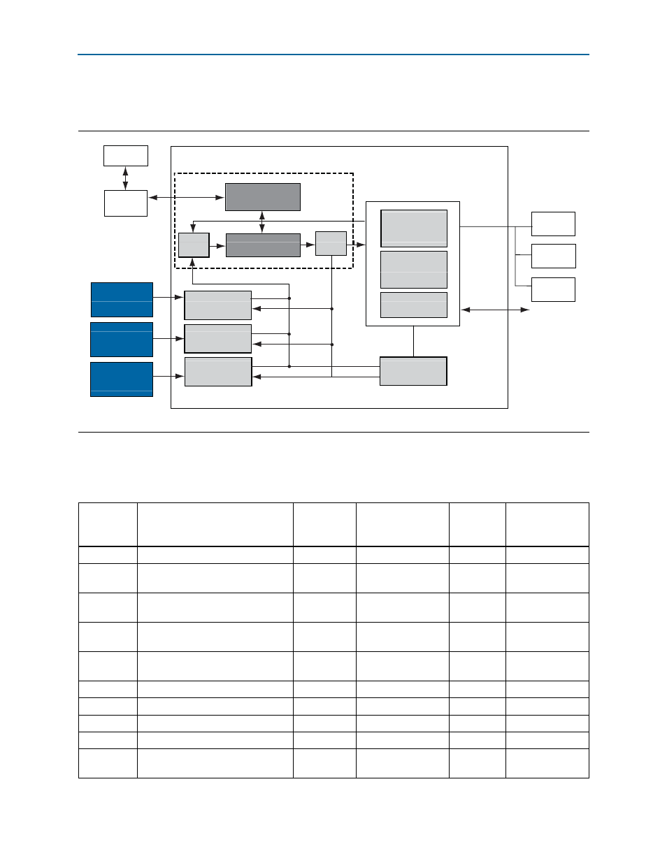
illustrates the MAX II CPLD EPM2210 System Controller's functionality
and external circuit connections as a block diagram.
lists the I/O signals present on the MAX
II CPLD EPM2210 System
Controller. The signal names and functions are relative to the MAX
II device (U72).
Figure 2–3. MAX II CPLD EPM2210 System Controller Block Diagram
MAX1619
Controller
Information
Register
EMB
Blaster
MAX II Device
Si5338
Controller
SLD-HUB
PFL
FSM BUS
Power
Measure
Results
Virtual-JTAG
PC
Temperature
Measure
Results
FPGA
LTC2418
Controller
FLASH
Decoder
Encoder
GPIO
JTAG Control
SRAM
Control
Register
Fast Configuration
Downloader
Si5338
Programmable
Oscillator
Table 2–5. MAX II CPLD EPM2210 System Controller Device Pin-Out (Part 1 of 6)
EPM2210
Pin Number
Description
Type
Schematic Signal
Name
Stratix IV
GT Device
Pin Name
Other
Connections
U72.U18
MAX_Stratix Bridge signal
Bidirectional
MS_FLASH_BYTEN
U44.AP34
—
U72.U16
Si5338 serial 2-wire clock for
memory PLL
Output
SI5338_MEM_SCL
—
U22.12, U56.12
U72.R13
Si5338 serial 2-wire data for
memory PLL
Bidirectional
SI5338_MEM_SDA
—
U22.19, U56.19
U72.V15
Si5338 serial 2-wire clock for
transceiver PLL
Output
SI5338_PLL_SCL
—
U21.12
U72.P13
Si5338 serial 2-wire data for
transceiver PLL
Bidirectional
SI5338_PLL_SDA
—
U21.19
U72.U14
EDC serial 2-wire clock
Output
EDC_SCL
—
U32.J1, U34.6
U72.N12
EDC serial 2-wire data
Bidirectional
EDC_SDA
—
U32.H1, U34.5
U72.T14
EDC write protect
Output
EDC_WP
—
U34.7
U72.V12
50-MHz oscillator clock enable
Output
CLK50_EN
—
X3.1
U72.C2
Dual frequency control signal for
SFP+ interface clocks.
Output
CLK_SFP_SEL
—
U46.2