Lcd –32 – Altera 100G Development Kit, Stratix IV GT Edition User Manual
Page 40
2–32
Chapter 2: Board Components
General User Input/Output
100G Development Kit, Stratix IV GT Edition Reference Manual
September 2010
Altera Corporation
lists the component references and the manufacturing information.
LCD
The development board contains a single 14-pin 0.1" pitch dual-row header that
interfaces to a 16 character × 2 line Lumex LCD display. The LCD has a 14-pin
receptacle that mounts directly to the board's 14-pin header, so it can be easily
removed for access to components under the display. You can also use the header for
debugging or other purposes.
Table 2–21
summarizes the LCD pin assignments. The signal names and directions are
relative to the MAX II CPLD.
shows the LCD pin definitions, and is an excerpt from the Lumex data
sheet.
f
For more information such as timing, character maps, interface guidelines, and other
related documentation, visi
SW4.7
User-Defined DIP switch
connected to FPGA device.
FPGA_USER_DIPSW6
2.5-V CMOS
R14
—
SW4.8
FPGA_USER_DIPSW7
H10
—
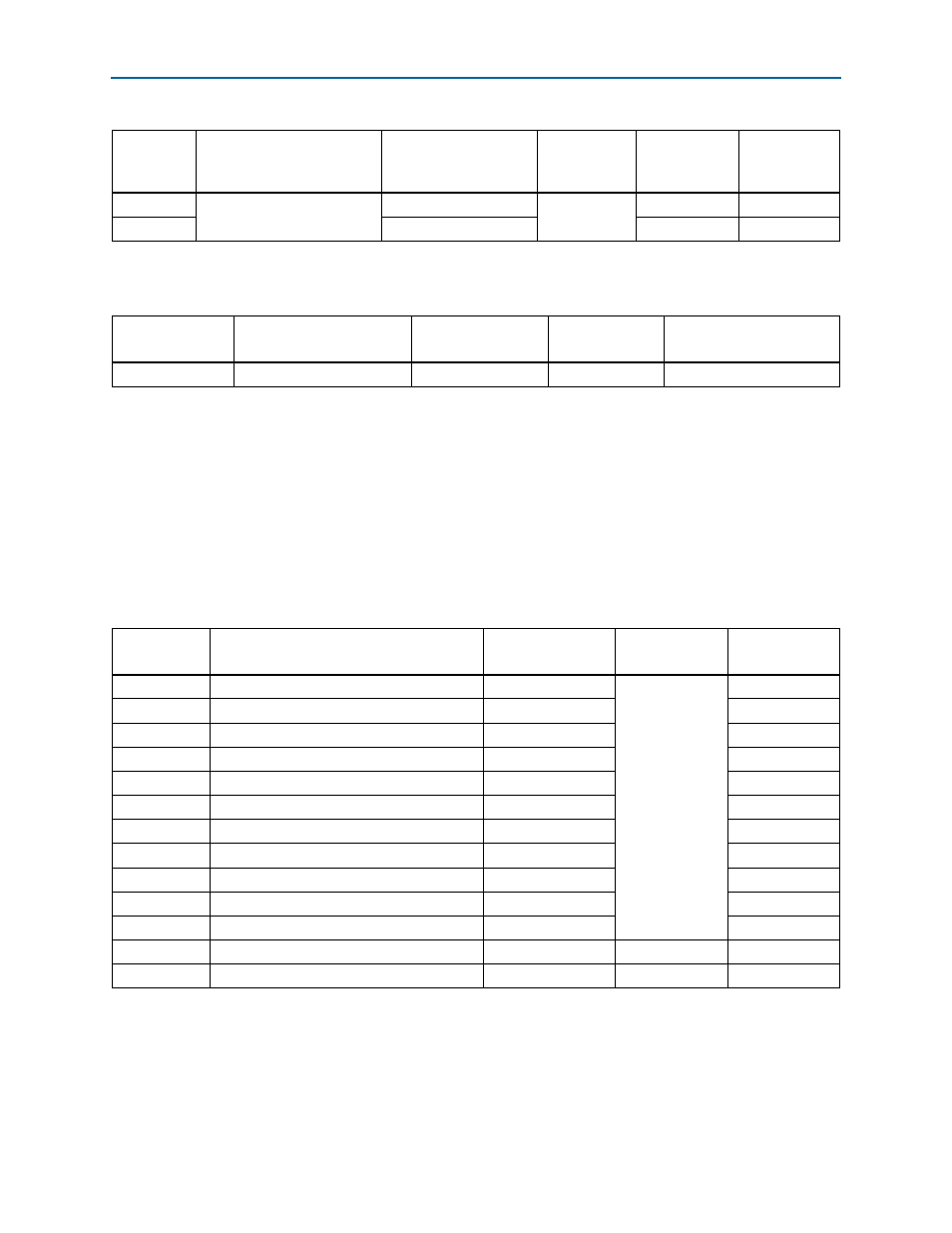
Table 2–19. User-Defined DIP Switch Schematic Signal Names and Functions
Board
Reference
Description
Schematic
Signal Name
I/O Standard
Stratix IV GT
Device
Pin Number
Other
Connections
Table 2–20. Component Reference Input and Ouput Devices
Board Reference
Device Description
Manufacturer
Manufacturer
Part Number
Manufacturer Website
SW3, SW4
DIP switch
Grayhill Corporation
76SB08ST
Table 2–21. LCD Pin Assignments, Schematic Signal Names, and Functions
Board
Reference
Description
Schematic
Signal Name
I/O Standard
Other
Connections
J59.7
LCD data bus 0
LCD_DATA0
2.5-V CMOS
U72.G6
J59.8
LCD data bus 1
LCD_DATA1
U72.H2
J59.9
LCD data bus 2
LCD_DATA2
U72.G5
J59.10
LCD data bus 3
LCD_DATA3
U72.H3
J59.11
LCD data bus 4
LCD_DATA4
U72.G4
J59.12
LCD data bus 5
LCD_DATA5
U72.G1
J59.13
LCD data bus 6
LCD_DATA6
U72.F6
J59.14
LCD data bus 7
LCD_DATA7
U72.G2
J59.4
LCD data or control signal
LCD_D_Cn
U72.G7
J59.5
LCD write enable
LCD_WEn
U72.J3
J59.6
LCD chip select
LCD_CSn
U72.H1
J59.1
Power
VCC
5.0-V
—
J59.2, J59.3
Ground
VSS
—
—