Altera 100G Development Kit, Stratix IV GT Edition User Manual
Page 62
2–54
Chapter 2: Board Components
Components and Interfaces
100G Development Kit, Stratix IV GT Edition Reference Manual
September 2010
Altera Corporation
U29.A7
Data bus
DDR3C_DQ28
U44.C26
—
U29.A2
Data bus
DDR3C_DQ29
U44.A30
—
U29.B8
Data bus
DDR3C_DQ30
U44.B26
—
U29.A3
Data bus
DDR3C_DQ31
U44.A29
—
U28.G3
Data strobe N byte lane 0
DDR3C_DQS_N0
U44.N26
—
U28.F3
Data strobe P byte lane 0
DDR3C_DQS_P0
U44.P26
—
U28.B7
Data strobe N byte lane 1
DDR3C_DQS_N1
U44.G28
—
U28.C7
Data strobe P byte lane 1
DDR3C_DQS_P1
U44.H28
—
U29.G3
Data strobe N byte lane 2
DDR3C_DQS_N2
U44.F27
—
U29.F3
Data strobe P byte lane 2
DDR3C_DQS_P2
U44.F28
—
U29.B7
Data strobe N byte lane 3
DDR3C_DQS_N3
U44.B28
—
U29.C7
Data strobe P byte lane 3
DDR3C_DQS_P3
U44.C28
—
U29.K1, U28.K1
On-die termination
DDR3C_ODT
U44.F33
—
U29.J3, U28.J3
Row address select
DDR3C_RASN
U44.U30
—
U29.T2, U28.T2
Reset
DDR3C_RSTN
U44.G39
—
U29.L3, U28.L3
Write enable
DDR3C_WEN
U44.V30
—
DDR3D Interface
U30.N3, U31.N3
Address bus
DDR3D_A0
U44.V31
—
U30.P7, U31.P7
Address bus
DDR3D_A1
U44.C24
—
U30.P3, U31.P3
Address bus
DDR3D_A2
U44.N34
—
U30.N2, U31.N2
Address bus
DDR3D_A3
U44.W30
—
U30.P8, U31.P8
Address bus
DDR3D_A4
U44.C23
—
U30.P2, U31.P2
Address bus
DDR3D_A5
U44.J37
—
U30.R8, U31.R8
Address bus
DDR3D_A6
U44.A23
—
U30.R2, U31.R2
Address bus
DDR3D_A7
U44.K37
—
U30.T8, U31.T8
Address bus
DDR3D_A8
U44.B23
—
U30.R3, U31.R3
Address bus
DDR3D_A9
U44.L36
—
U30.L7, U31.L7
Address bus
DDR3D_A10
U44.F23
—
U30.R7, U31.R7
Address bus
DDR3D_A11
U44.D25
—
U30.N7, U31.N7
Address bus
DDR3D_A12
U44.F25
—
U30.M2, U31.M2
Bank address bus
DDR3D_BA0
U44.P32
—
U30.N8, U31.N8
Bank address bus
DDR3D_BA1
U44.A24
—
U30.M3, U31.M3
Bank address bus
DDR3D_BA2
U44.R30
—
U30.K3, U31.K3
Column address select
DDR3D_CASN
U44.F24
—
U30.K7, U31.K7
Clock input N
DDR3D_CK_N
U44.J39
—
U30.J7, U31.J7
Clock input P
DDR3D_CK_P
U44.K39
—
U30.K9, U31.K9
Clock enable
DDR3D_CKE
U44.A22
—
U30.L2, U31.L2
Chip select
DDR3D_CSN
U44.L25
—
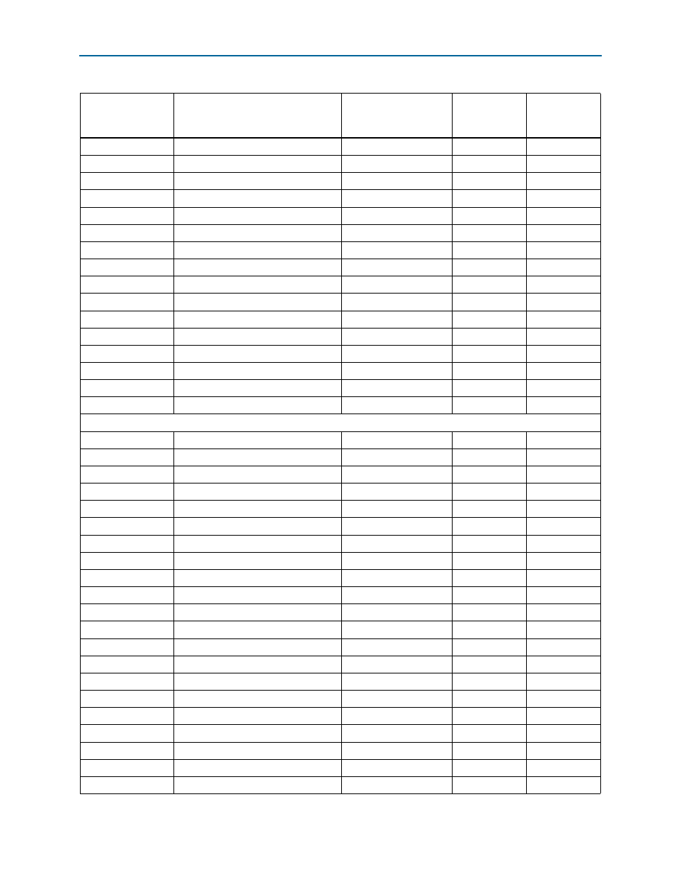
Table 2–37. DDR3 Interface Pin Assignments, Schematic Signal Names, and Functions (Part 6 of 8)
Board Reference
Description
Schematic
Signal Name
Stratix IV GT
Device
Pin Name
Other
Connections