Altera 100G Development Kit, Stratix IV GT Edition User Manual
Page 33
Chapter 2: Board Components
2–25
Clock Circuitry
September 2010
Altera Corporation
100G Development Kit, Stratix IV GT Edition Reference Manual
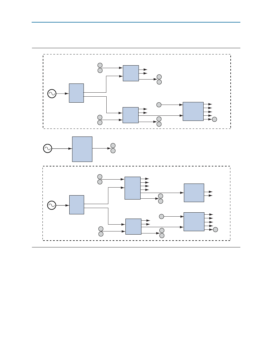
Figure 2–7
shows the Stratix IV GT 100G development board clock tree structure.
The clock distribution path is done using the board settings DIP switch (SW2). This
DIP switch is located near the differential clock buffer B. Refer to
switch settings and descriptions. The USB_DISABLEn DIP switch is connected to the
MAX II device and controls the traffic that passes through the USB connector.
Figure 2–8. Stratix IV GT 100G Development Board Clock Tree Structure
Reference
Clock
PLL
LVPECL
to
LVDS
Differential
Clock
Single-Ended
Clock
25 MHz
LVCMOS
644 MHz
Reference
Clock
PLL
Differential
Clock
LVPECL
25 MHz
(Same
oscillator as
in Clock A)
Divide-by-4
Circuit
LVDS
Clock A
Clock B
LVDS
LVDS
LVDS
LVDS
LVDS
LVDS
LVDS
LVDS
LVDS
LVDS
Interlaken Side
Line Side
LVPECL
LVPECL
Single-Ended
Clock
LVCMOS
XFP
CFP
Si5338
(Part A)
Si5338
(Part B)