Altera 100G Development Kit, Stratix IV GT Edition User Manual
Page 35
Chapter 2: Board Components
2–27
Clock Circuitry
September 2010
Altera Corporation
100G Development Kit, Stratix IV GT Edition Reference Manual
U22.22
DDR3 PLL clock D
DDR3_CLKD_N
LVDS
P23
—
U56.9
QDR II PLL clock A
QDR2_CLKA_P
AK21
—
U56.10
QDR II PLL clock A
QDR2_CLKA_N
AL22
—
U56.13
QDR II PLL clock B
QDR2_CLKB_P
AJ22
—
U56.14
QDR II PLL clock B
QDR2_CLKB_N
AK22
—
U56.17
QDR II PLL clock C
QDR2_CLKC_P
AJ24
—
U56.18
QDR II PLL clock C
QDR2_CLKC_N
AK23
—
U56.21
QDR II PLL clock D
QDR2_CLKD_P
AK24
—
U56.22
QDR II PLL clock D
QDR2_CLKD_N
AL25
—
U18.4
SMA input for differential clock buffer B
SMA_DIFF_CLKIN_P1
—
J19.1
U18.5
SMA input for differential clock buffer B
SMA_DIFF_CLKIN_N1
—
J26.1
U18.15
Differential clock buffer B to FPGA
fabric
BUFFB3_SE_CLK_P
—
J17.5
U18.14
Differential clock buffer B to FPGA
fabric
BUFFB3_SE_CLK_N
—
J17.6
U18.12
Differential clock buffer B to SMA
BUFFB_CLK_P
—
J20.1
U18.11
Differential clock buffer B to SMA
BUFFB_CLK_N
—
J27.1
U20.6
SMA input for reference clock buffer B
REFCLK_OSC_P
—
J18.1
U20.7
SMA input for reference clock buffer B
REFCLK_OSC_N
—
J25.1
U20.3
Reference clock buffer B to transceivers
REFCLK_QL0_P
BB2
—
U20.4
REFCLK_QL0_N
BB1
—
U20.18
REFCLK_QL1_P
AK2
—
U20.19
REFCLK_QL1_N
AK1
—
U20.12
REFCLK_QL2_P
V2
—
U20.13
REFCLK_QL2_N
V1
—
U20.10
REFCLK_QL3_P
F2
—
U20.11
REFCLK_QL3_N
F1
—
U17.4
SMA input for single-ended clock buffer
B
SE_CLKINB_SMA
2.5-V
CMOS
—
J14.1
U17.23
Single-ended clock buffer B
SE_CLKB_L
V7
—
U17.21
SE_CLKB_R
AD39
—
U17.19
SE_CLKB_MAX
—
U72.K6
U17.13
SE_CLKOUTB_SMA
—
J15.1
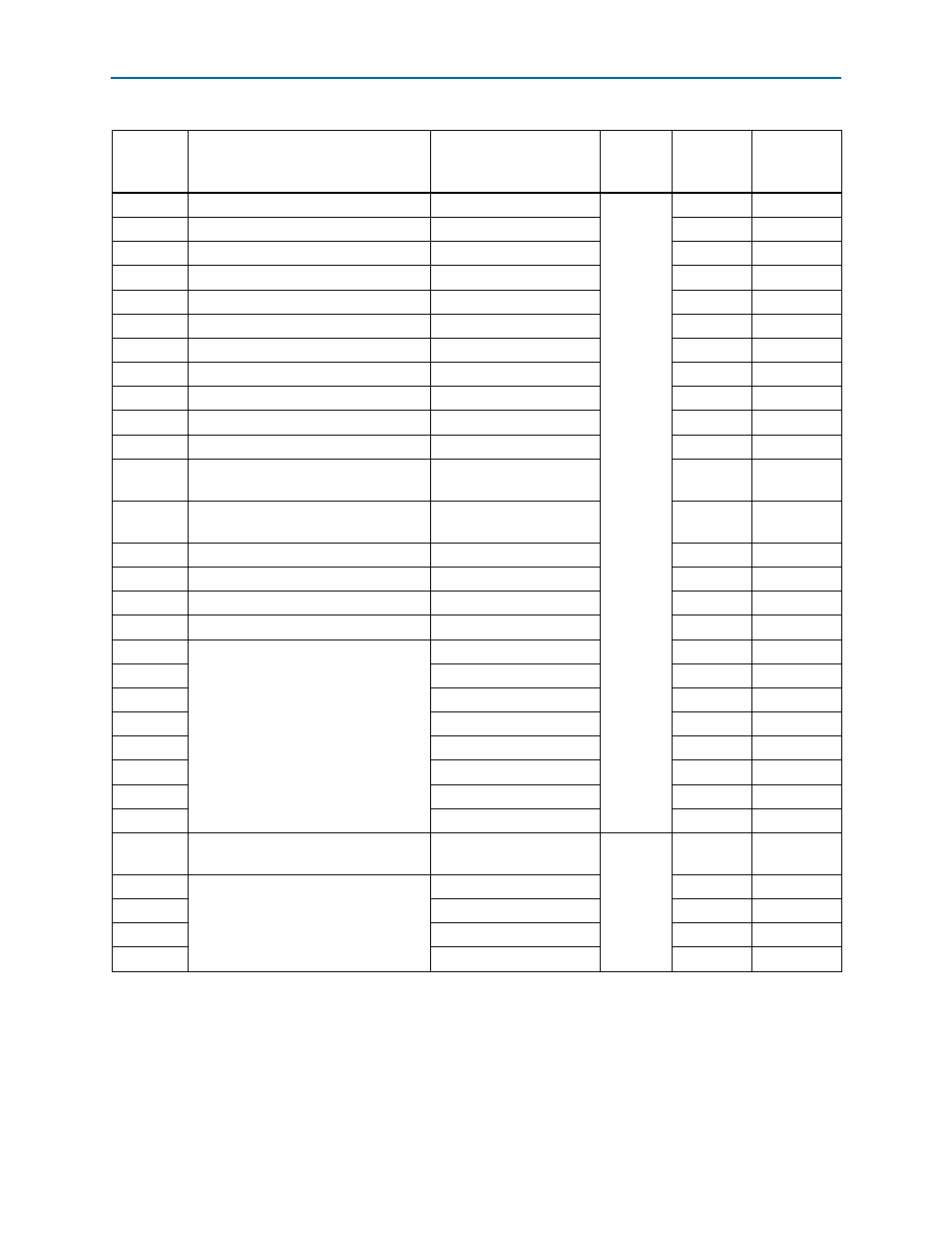
Table 2–14. Spread Spectrum Configuration DIP Switch Pin-Out (SW2) (Part 2 of 3)
Board
Reference
Description
Schematic
Signal Name
I/O
Standard
Stratix IV
GT Device
Pin Name
Other
Connections