Flash memory, Flash memory –33, Table 2–23 – Altera 100G Development Kit, Stratix IV GT Edition User Manual
Page 41
Chapter 2: Board Components
2–33
Flash Memory
September 2010
Altera Corporation
100G Development Kit, Stratix IV GT Edition Reference Manual
1
The particular model used on this board does not have a backlight and therefore the
LCD drive pin is not connected.
lists the LCD component references and the manufacturing information.
Flash Memory
The board features a Numonyx PC28F00AM29EWL 1-Gb CFI-compliant NOR-type
flash memory device, which stores configuration files for the FPGA. Both MAX II
CPLD (U72) and FPGA (U44) devices can access the flash. The MAX II accesses are for
FPP configuration of the FPGA using the PFL Megafunction. The FPGA access to the
flash’s user space is provided for embedded NIOS applications.
provides the pin-out information of the flash memory interface to the
FPGA. The signal direction is with respect to the FPGA device.
Table 2–22. LCD Pin Definitions and Functions
Pin Number
Symbol
Level
Function
1
V
DD
—
Power supply
5 V
2
V
SS
—
GND (0 V)
3
V
0
—
For LCD drive
4
RS
H/L
Register select signal
H: Data input
L: Instruction input
5
R/W
H/L
H: Data read (module to MPU)
L: Data write (MPU to module)
6
E
H, H to L
Enable
7–14
DB0–DB7
H/L
Data bus, software selectable 4-bit or 8-bit mode
Table 2–23. LCD Component References And The Manufacturing Information
Board
Reference
Device Description
Manufacturer
Manufacturer
Part Number
Manufacturer
Website
J59
2×16 character display, 5×8 dot matrix
Lumex Inc.
LCM-S01602DSR/C
2×7 pin, 100 mil, vertical header
Samtec
TSM-107-01-G-DV
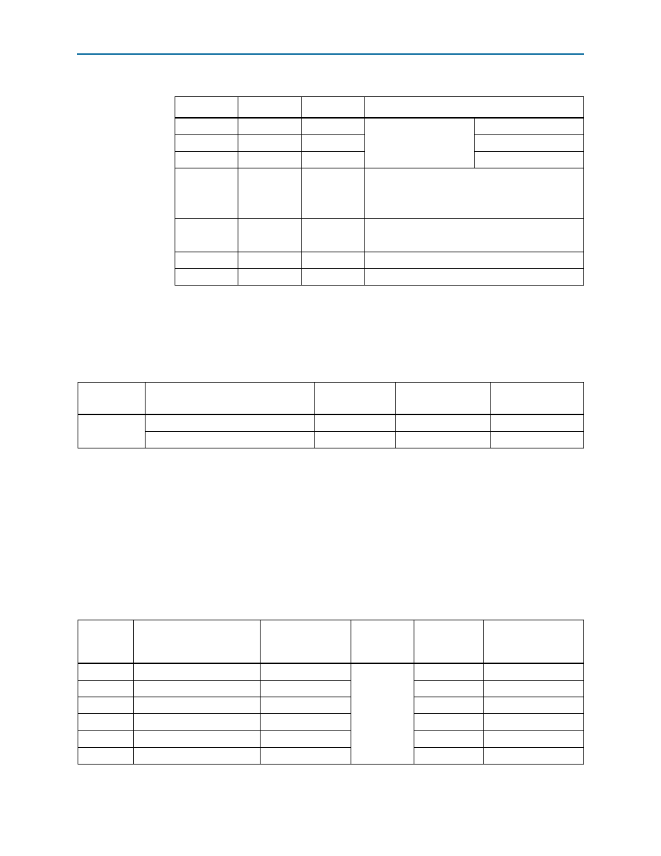
Table 2–24. Flash Memory Pin-Out (Part 1 of 3)
Board
Reference
Description
Schematic
Signal Name
I/O Standard
Stratix IV GT
Device
Pin Name
Other Connections
U65.E2
Flash address bus bit 1
FSM_A1
2.5-V CMOS
AR6
—
U65.D2
Flash address bus bit 2
FSM_A2
AL13
U57.R6, U72.E11
U65.C2
Flash address bus bit 3
FSM_A3
AV6
U57.P6, U72.B13
U65.A2
Flash address bus bit 4
FSM_A4
AN6
U57.A2, U72.A12
U65.B2
Flash address bus bit 5
FSM_A5
AA14
U57.A10, U72.A13
U65.D3
Flash address bus bit 6
FSM_A6
AN39
U57.B2, U72.C13