Ssram, Ssram –35 – Altera 100G Development Kit, Stratix IV GT Edition User Manual
Page 43
Chapter 2: Board Components
2–35
SSRAM
September 2010
Altera Corporation
100G Development Kit, Stratix IV GT Edition Reference Manual
shows the flash memory map.
1
For more information on the flash memory map, refer to th
.
lists the flash memory device component reference and manufacturing
information.
SSRAM
The Synchronous Static Random Access Memory (SSRAM) device consists of a single
standard synchronous SRAM, providing 2 Mbyte with a 36-bit data bus. This device is
part of the shared FSM bus, which connects to the flash memory, SSRAM, and the
MAX
II CPLD EPM2210 System Controller.
The device speed is 250 MHz single-data-rate. There is no minimum speed for this
device. The theoretical bandwidth of this 32-bit memory interface is 8.0 Gbps for
continuous bursts. The read latency for any address is two clocks, in which at
250 MHz, the latency is 10 ns and at 50 MHz, the latency is 40 ns. The write latency is
one clock.
U65.G2
Flash output enable
FLASH_OEn
2.5-V CMOS
—
U72.E9
U65.A5
Flash write enable
FLASH_WEn
—
U72.A8
U65.B4
Flash write protect
FLASH_WPn
—
—
U65.A4
Flash ready
FLASH_RDYBSYn
—
U72.B9
U65.F7
Flash byte enable
FLASH_BYTEn
—
U72.A9
Table 2–24. Flash Memory Pin-Out (Part 3 of 3)
Board
Reference
Description
Schematic
Signal Name
I/O Standard
Stratix IV GT
Device
Pin Name
Other Connections
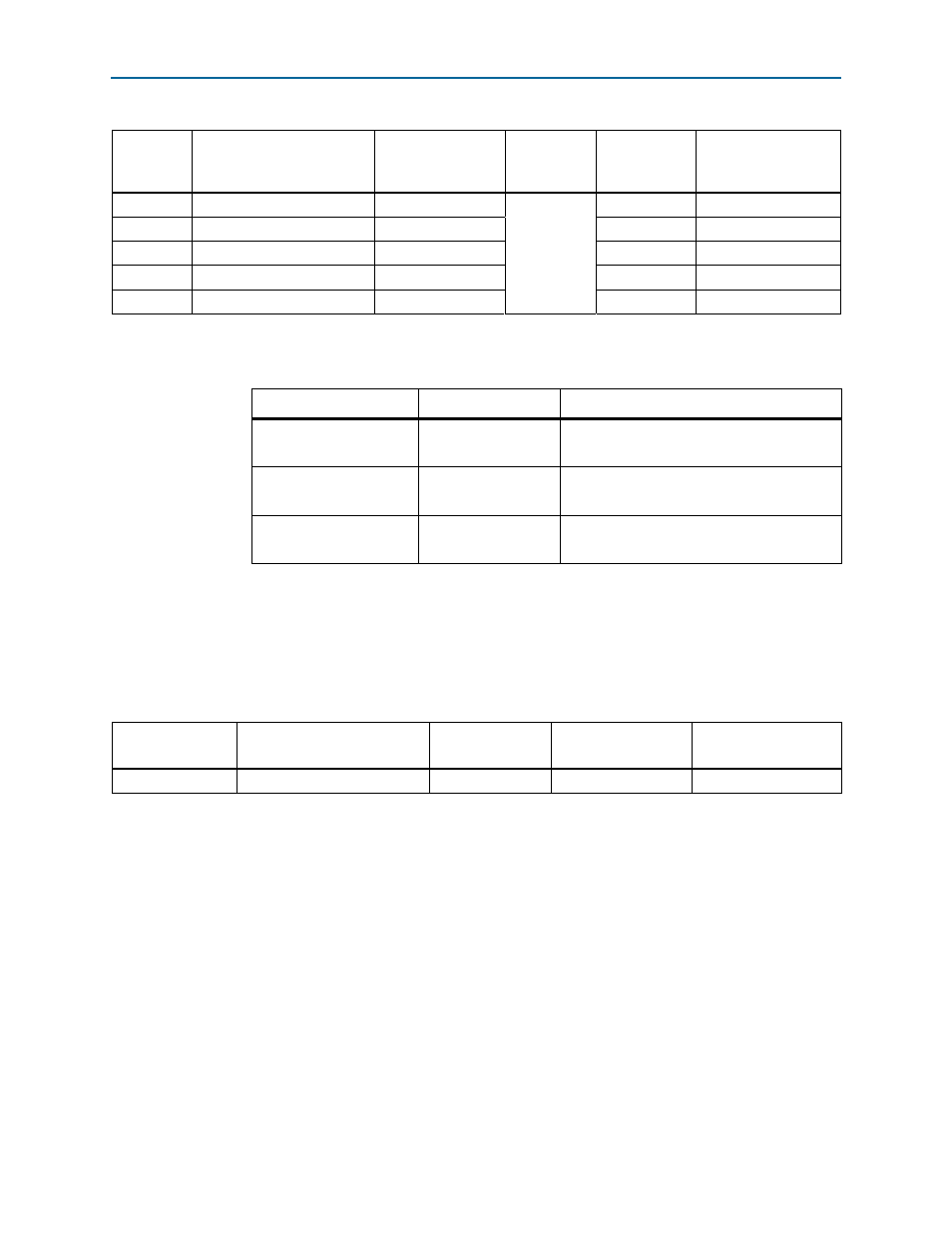
Table 2–25. Flash Memory Map
Name
Size (MB)
Address
Reserved
128
0x07FF.FFFF
0x07FE.0000
USER
40
0x07FD.FFFF
0x052C.0000
FACTORY
10
0x052B.FFFF
0x0486.0000
Table 2–26. Flash Memory Component References And The Manufacturing Information
Board Reference
Description
Manufacturer
Manufacturing
Part Number
Manufacturer
Website
U65
1-Gb NOR-type flash
Numonyx
PC28F00AM29EWL