Altera 100G Development Kit, Stratix IV GT Edition User Manual
Page 52
2–44
Chapter 2: Board Components
Components and Interfaces
100G Development Kit, Stratix IV GT Edition Reference Manual
September 2010
Altera Corporation
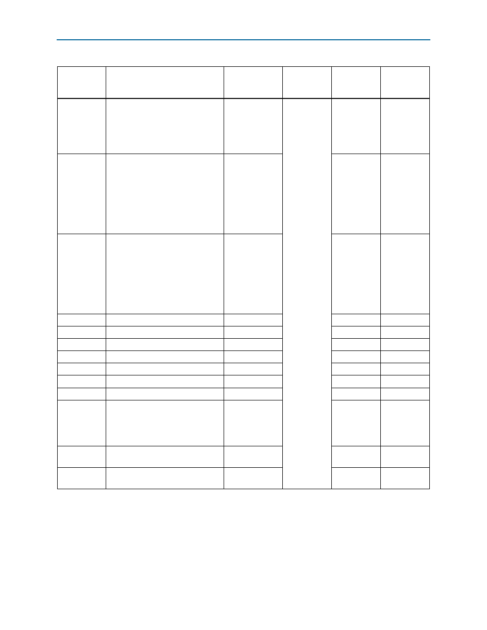
J37.30
Programmable control 1 set via
MDIO and MSA for TX and RX IC
reset (TRXIC_RSTn)
0: Reset
1 or NC: Enabled or not in use
CFP_PRG_CNTL1
1.2-V PCML
U14
—
J37.31
Programmable control 2 set via
MDIO and MSA for hardware power
interlock (LSB).
00: < 8 W
01: < 16 W
10: < 24 W
11 or NC: > 24 W or not in use
CFP_PRG_CNTL2
U13
—
J37.32
Programmable control 3 set via
MDIO and MSA for hardware power
interlock (MSB).
00: < 8 W
01: < 16 W
10: < 24 W
11 or NC: > 24 W or not in use
CFP_PRG_CNTL3
J8
—
J37.46
MDIO port address
CFP_T_PRTADR0
K8
—
J37.45
MDIO port address
CFP_T_PRTADR1
L9
—
J37.44
MDIO port address
CFP_T_PRTADR2
V14
—
J37.43
MDIO port address
CFP_T_PRTADR3
V15
—
J37.42
MDIO port address
CFP_T_PRTADR4
J7
—
J37.147
Input reference clock
CFP_REFCLK_N
—
U16.14
J37.146
Input reference clock
CFP_REFCLK_P
—
U16.15
J37.40
Receiver loss of optical signal on any
channel.
0: Normal condition.
1: Signal loss.
CFP_RX_LOS
F8
—
J37.77
Only used for optical waveform
testing.
CFP_RX_MCLK_N
—
J51.1
J37.76
Only used for optical waveform
testing.
CFP_RX_MCLK_P
—
J44.1
Table 2–33. CFP Interface Pin Assignments, Schematic Signal Names, and Functions (Part 3 of 3)
Board
Reference
Description
Schematic
Signal Name
i/O Standard
Stratix IV GT
Device
Pin Name
Other
Connections