Development board block diagram, Handling the board – Altera 100G Development Kit, Stratix IV GT Edition User Manual
Page 7
Chapter 1: Overview
1–3
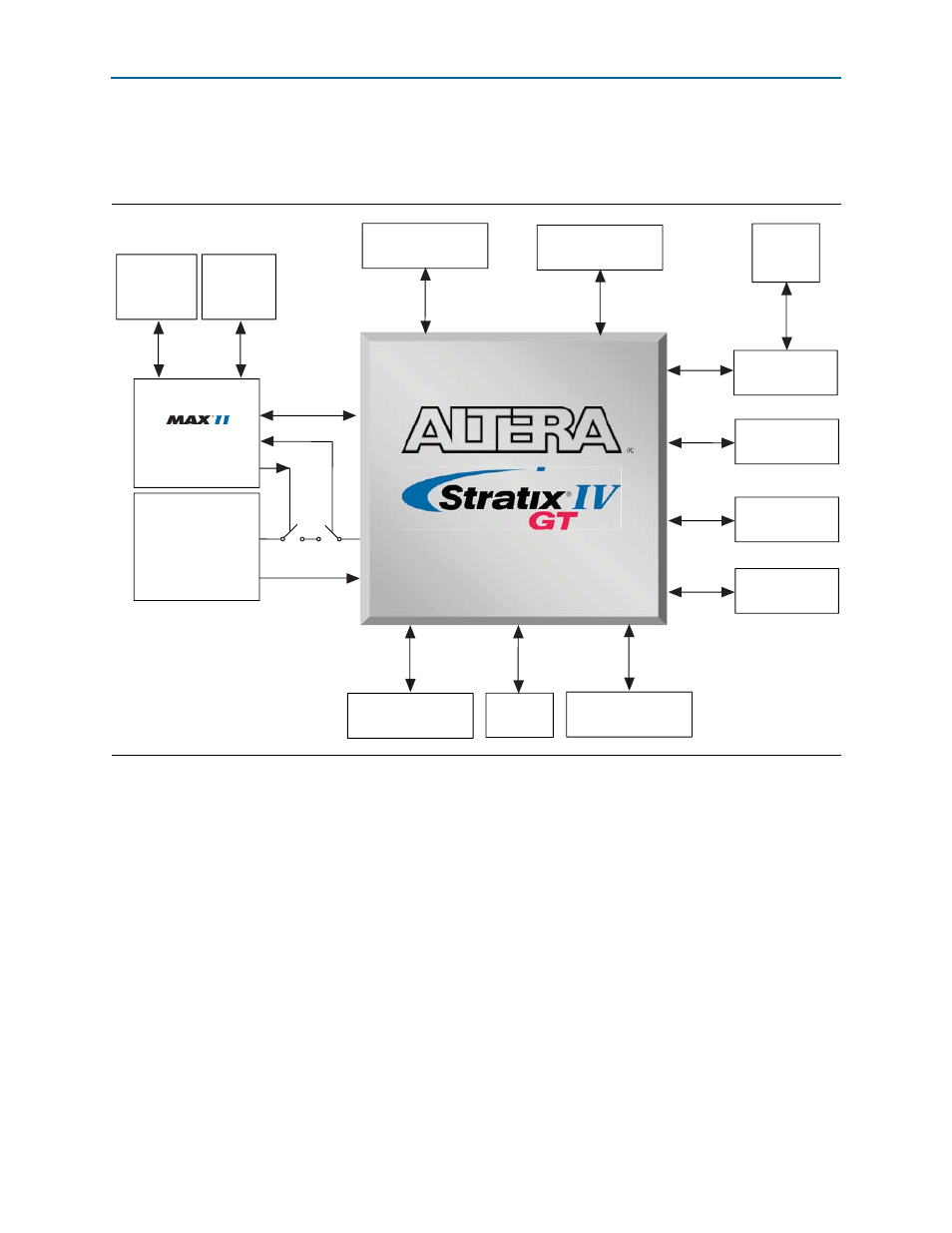
Development Board Block Diagram
September 2010
Altera Corporation
100G Development Kit, Stratix IV GT Edition Reference Manual
Development Board Block Diagram
shows the block diagram of the Stratix IV GT 100G development board.
Handling the Board
When handling the board, it is important to observe the following static discharge
precaution:
c
Without proper anti-static handling, the board can be damaged. Therefore, use
anti-static handling precautions when touching the board.
The Stratix IV GT 100G development board must be stored between –40º C and
100º C. The recommended operating temperature is between 0º C and 55º C.
Figure 1–1. Stratix IV GT 100G Development Board Block Diagram
EP4S100G5F1932
CPLD
(x32)
User LEDs,
Push-Buttons
USB
Blaster
10/100/1000
Ethernet
RJ45
Jack
4 MB QDR II
(x18)
64 MB
SRAM
Flash
CFP
QSFP
Clocks
& PLL
DDR3 SDRAM
(x32)
SFP+
SFP+
with EDC
Interlaken