Altera 100G Development Kit, Stratix IV GT Edition User Manual
Page 12
2–4
Chapter 2: Board Components
Board Overview
100G Development Kit, Stratix IV GT Edition Reference Manual
September 2010
Altera Corporation
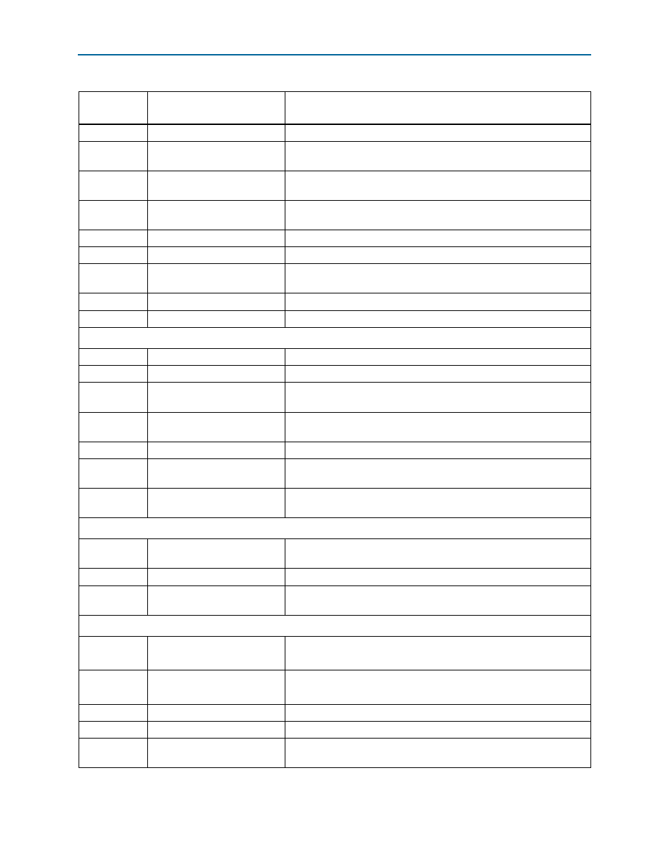
U13
LVPECL to LVDS buffer
644.53125MHz LVDS clock buffer.
U15, U18, U19
Differential to LVDS clock
buffer
Differential clock buffer (2 to 4) distributed to CMU and dedicated
differential clock inputs on the vertical banks of the FPGA.
U16
Differential divide-by-4 clock
divider
Divide-by-4 clock circuit to provide the required clock to EDC and CFP.
U20
Differential to LVDS clock
buffer
Differential clock buffer (2 to 6) distributed to CMU of the FPGA and to
clock dividers for the optical clock.
U21, U22, U56 External programmable PLLs
On-board programmable PLL clock source with buffers.
U14, U17
Single-ended clock buffer
Single-ended clock buffer provided to each side of the FPGA.
X1
644.53125-MHz LVPECL
oscilator
644.53-MHz clock to the FPGA transceivers.
X3
50-MHz oscillator
50-MHz Nios CPU clock (CMOS).
Y1, Y2, Y3
25-MHz crystal clock
25-MHz reference clock for external PLLs.
General User Input and Output
D21–D24
User LEDs
Four green LEDs for the MAX II CPLD EPM2210 System Controller.
D28–D35
FPGA LEDs
Eight green LEDs for the FPGA.
J59
Character LCD
Connector which interfaces to the provided 16 character × 2 line LCD
module.
S1–S4
User push-buttons
User push-buttons connected to the MAX II CPLD EPM2210 System
Controller.
S5–S8
FPGA user push-buttons
User push-buttons connected to the Stratix IV GT device.
SW3
Bank of eight user DIP
switches
User DIP switches connected to the MAX II CPLD EPM2210 System
Controller.
SW4
Bank of eight user DIP
switches
User DIP switches connected to the FPGA.
Memory Devices
U28-U31,
U36-U39
DDR3 x16 port
4 x32 independent DDR3 memory port.
U47-U50
QDR II x18/x18 port
4 x18 independent (18-bit read and 18-bit write) QDR II memory port.
U65
Flash memory
Synchronous burst mode flash device which provides 1-Gb non-volatile
memory port.
Components and Interfaces
J34
QSFP_TX_P/_N[3:0]
QSFP_RX_P/_N[3:0]
QSFP XCVR interface (4-channels).
J37
CFP_TX_P/_N[9:0]
CFP_RX_P/_N[9:0]
CFP XCVR interface (10-channels).
J31
SFP+ interface
SFP+ XCVR interface port B.
J32
SFP+ interface with EDC
SFP+ XCVR interface port A.
J48
I/O connector
General purpose expansion connector with 10 user-definable I/Os
connected to the MAX II CPLD EPM2210 System Controller.
Table 2–1. Stratix IV GT 100G Development Board Components (Part 3 of 5)
Board
Reference
Type
Description