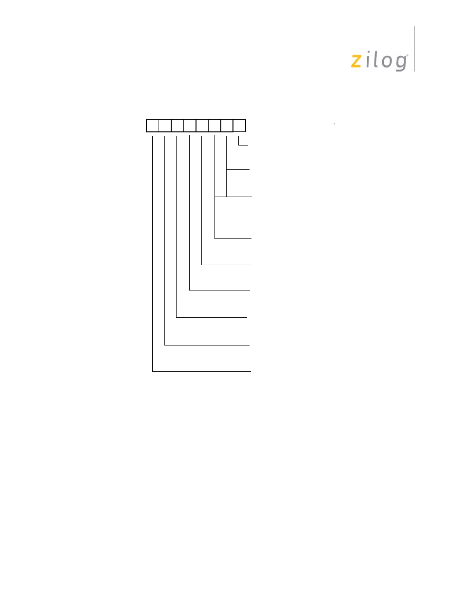
Figure 116 – Zilog Z86193 User Manual
Page 131

Z8
®
CPU
User Manual
UM001604-0108
Serial Input/Output
124
If the associated IRQ3 is enabled, an interrupt is generated. Bit 5 controls the clock phase
of the SPI. A 1 in bit 5 allows for receiving data on the clock’s falling edge and transmit-
ting data on the clock’s rising edge. A 0 allows receiving data on the clock’s rising edge
and transmitting on the clock’s falling edge. The SPI clock source is defined in bit 6. A 1
uses Timer0 output for the SPI clock, and a 0 uses TCLK for clocking the SPI. Finally, bit
7 determines whether the SPI is used as a Master or a Slave. A 1 puts the SPI into Master
mode and a 0 puts the SPI into Slave mode.
Figure 116. SPI Control Register
D7 D6 D5 D4 D3 D2 D1 D0
SCON (C) 02
CLK Divide (M)
00 TCLK/2
01 TCLK/4
10 TCLK/8
11 TCLK/16
DO SPI Port Enable (S)
0 SPI DO Port Enable
1 Do Port to I/O
0 Disable *
1 Enable
SPI Enable
0 Enable
1 Disable *
Compare Enable
0 Trans/Fall
1 Trans/Rise
Clock Phase
0 Reset
RxCharOverrun (S)
0 Reset
1 Char. Avail
RxCharAvail
1 Overrun
(M) Used with Bit D7 equal to 1
* Default setting after Reset
0 TCLK
1 Timer 0 Output
CLK Source
0 Slave
1 Master
Master Slave
(S) Used with Bit D7 equal to 0
- Z86233 Z86243 Z86733 Z86743 Z86C02 Z86C04 Z86C08 Z86C15 Z86C21 Z86C30 Z86C31 Z86C33 Z86C36 Z86C40 Z86C43 Z86C61 Z86C62 Z86C63 Z86C65 Z86C83 Z86C90 Z86C91 Z86C93 Z86C96 Z86E02 Z86E03 Z86E04 Z86E06 Z86E07 Z86E08 Z86E15 Z86E21 Z86E30 Z86E31 Z86E33 Z86E34 Z86E40 Z86E43 Z86E44 Z86E61 Z86E63 Z86E83 Z86K15 Z86L02 Z86L04 Z86L08 Z86L16 Z8E000 Z8E001 Z8PE003