6 test interface signals, Table 3.13 test interface signals, Test interface signals – Avago Technologies LSI53C895A User Manual
Page 104: Scsi signals, Section 3.6, “test interface signals, Test, Interface signals
3-16
Signal Descriptions
3.6 Test Interface Signals
describes Test Interface signals.
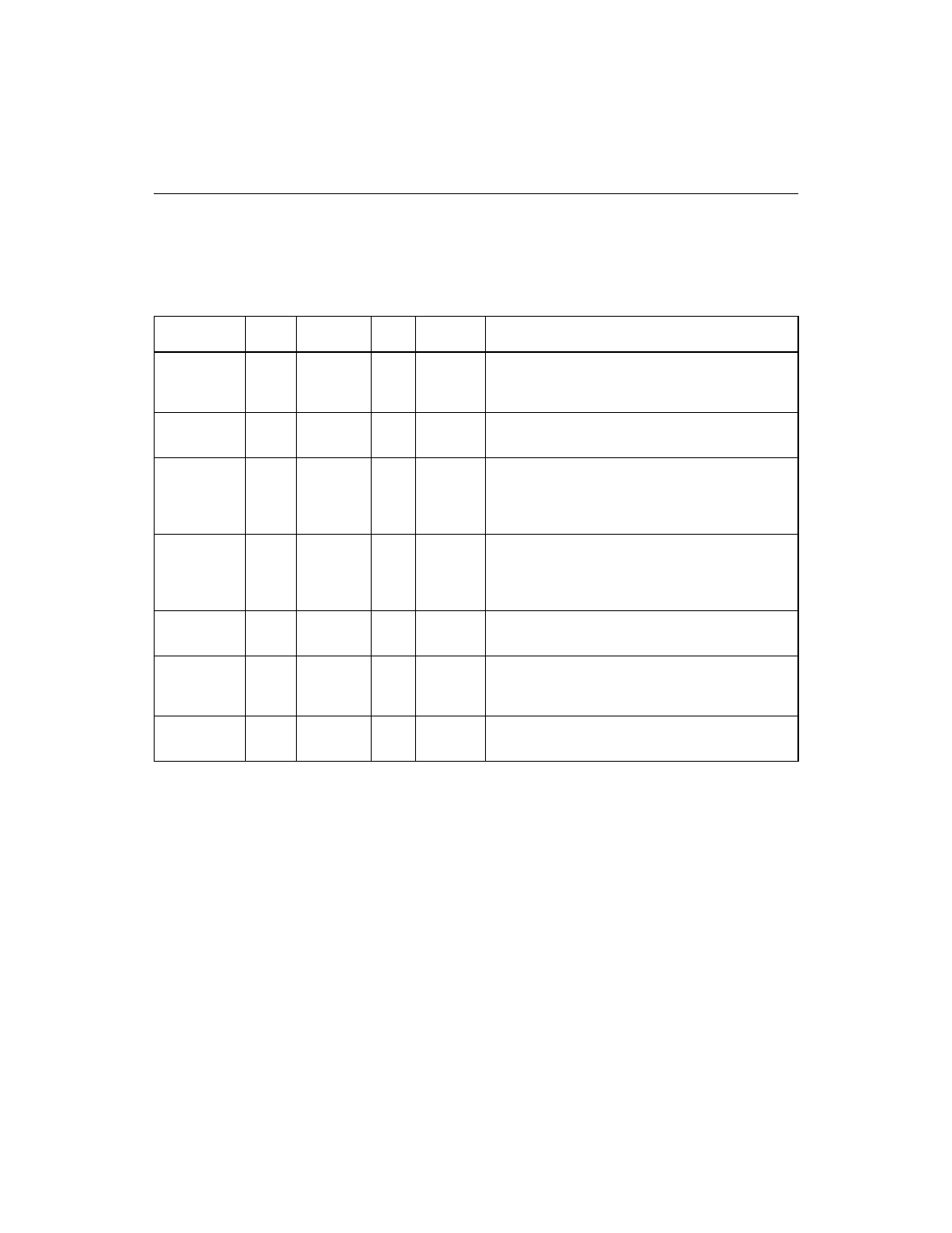
Table 3.13
Test Interface Signals
Name
PQFP
BGA Pos
Type Strength Description
TEST_HSC/
82
J19
I
N/A
Test Halt SCSI Clock. For LSI Logic pulled
HIGH internally. This signal can also cause a full
chip reset.
TCK
180
K1
I
N/A
Test Clock. This pin provides the clock for the
JTAG test logic.
TMS
181
L1
I
N/A
Test Mode Select. The signal received at TMS
is decoded by the TAP controller to control JTAG
test operations. This pin has a static
pull-down.
TDI
183
L3
I
N/A
Test Data In. Serial test instructions are
received by the JTAG test logic at this pin. This
pin has a static
pull-down.
TEST_RST/
178
K2
I
N/A
Test Reset. For test purposes only. Pulled HIGH
internally.
TDO
182
L2
O
4 mA
Test Data Out. This pin is the serial output for
test instructions and data from the JTAG test
logic.
TRST/
206
Y1
I
N/A
Test Reset. This pin provides a reset for JTAG
Test Logic. Pulled HIGH internally.