Bit address operating register/scripts ram write – Avago Technologies LSI53C895A User Manual
Page 281
Advertising
PCI and External Memory Interface Timing Diagrams
6-21
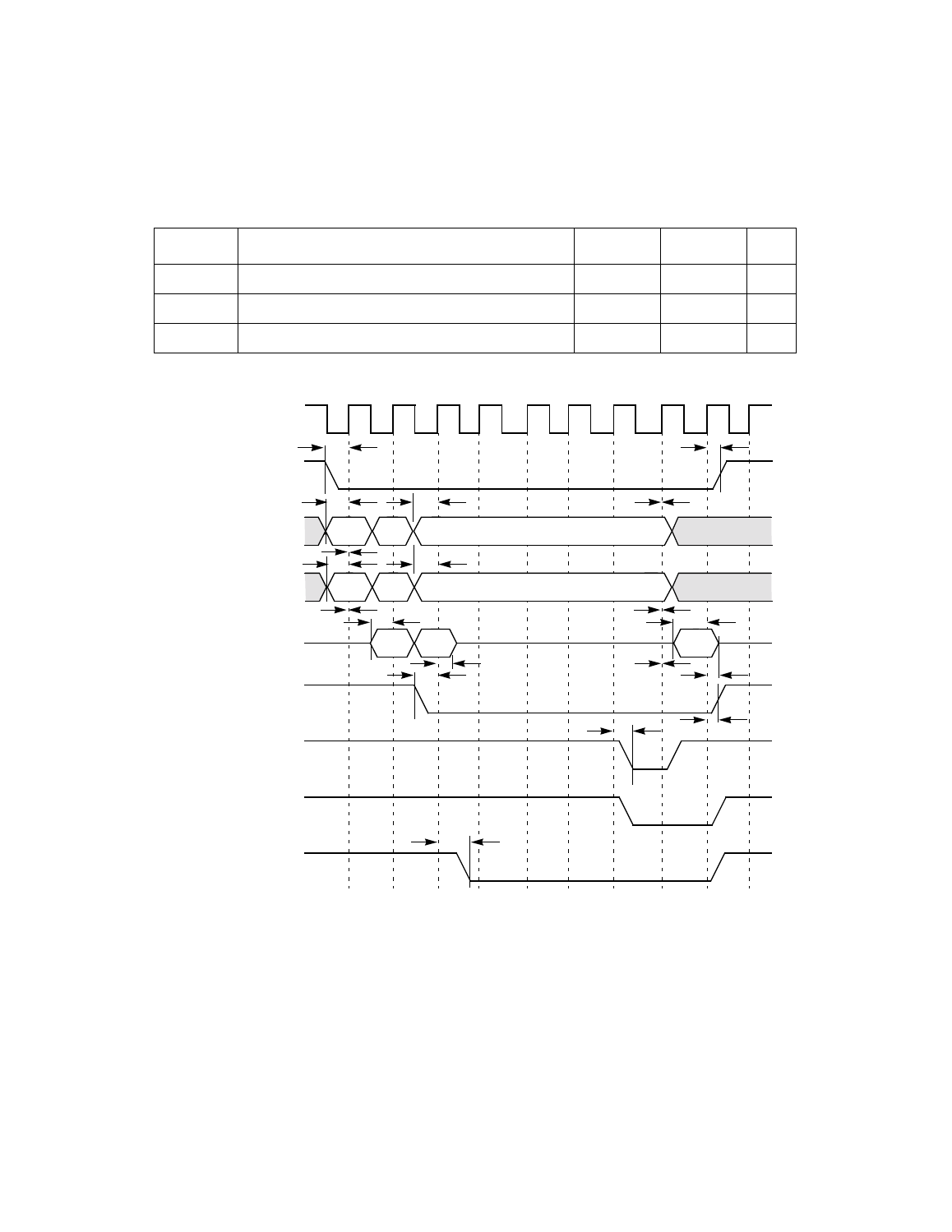
Figure 6.16 64-Bit Address Operating Register/SCRIPTS RAM Write
Table 6.23
64-Bit Address Operating Register/SCRIPTS RAM Write
Symbol
Parameter
Min
Max
Unit
t
1
Shared signal input setup time
7
–
ns
t
2
Shared signal input hold time
0
–
ns
t
3
CLK to shared signal output valid
–
11
ns
Bus
Addr
Lo
Addr
Hi
Data In
In
t
2
t
3
CLK
(Driven by System)
FRAME/
(Driven by Master)
AD
(Driven by Master)
C_BE/
(Driven by Master)
PAR
(Driven by Master)
IRDY/
(Driven by Master)
TRDY/
(Driven by LSI53C895A)
STOP/
(Driven by LSI53C895A)
DEVSEL/
(Driven by LSI53C895A)
CMD
Byte Enable
In
In
Dual
Addr
t
1
t
1
t
1
t
1
t
1
t
1
t
1
t
1
t
2
t
2
t
2
t
2
t
2
t
3
t
2
t
2
t
2
Advertising