Scsi test four (stest4), Scsi input, Data latch (sidl) – Avago Technologies LSI53C895A User Manual
Page 204: Scsi input data latch (sidl), Scsi, Input data latch (sidl), Scsi input data, Latch (sidl), Register: 0x52
4-96
Registers
Registers: 0x50–0x51
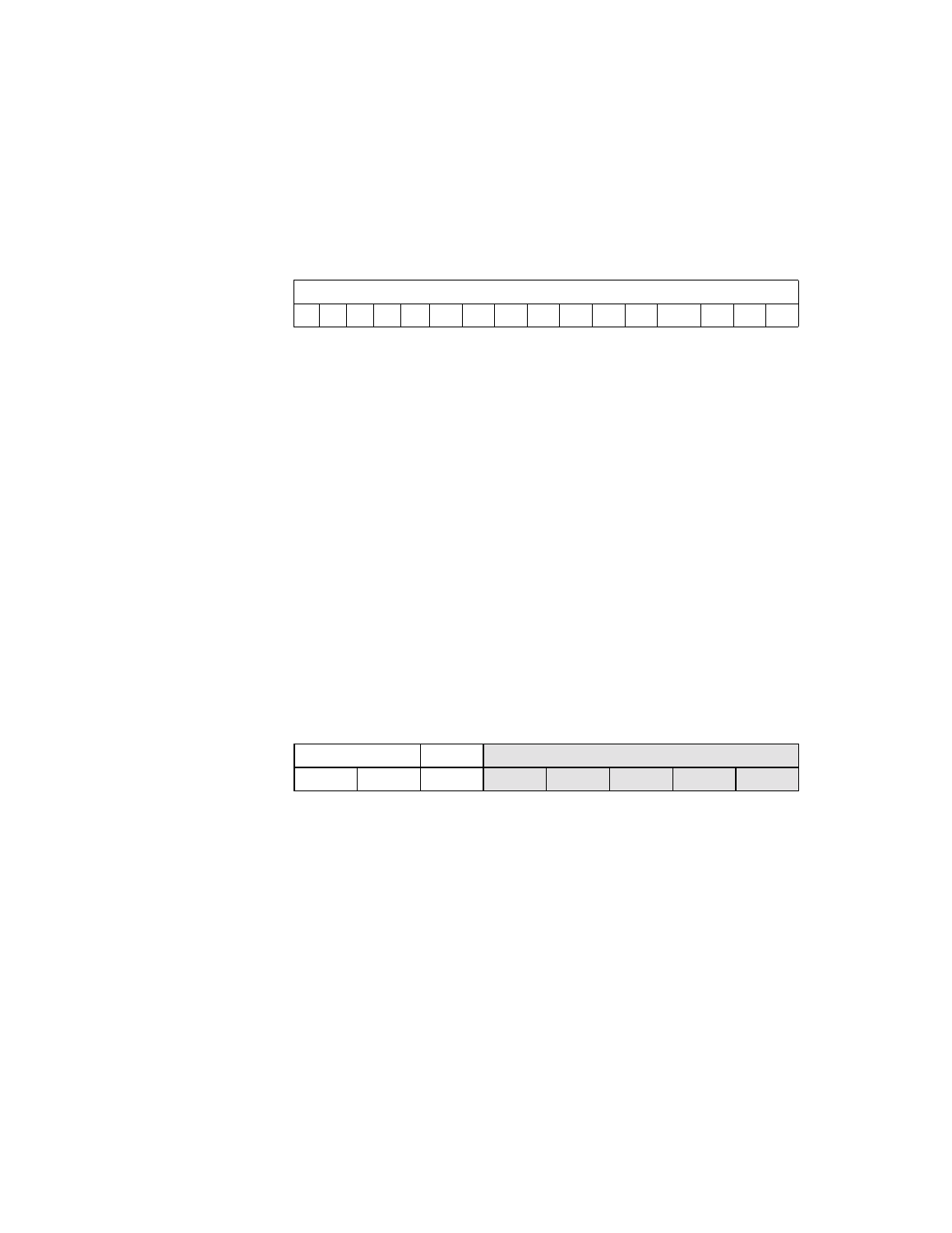
SCSI Input Data Latch (SIDL)
Read Only
SIDL
SCSI Input Data Latch
[15:0]
This register is used primarily for diagnostic testing,
programmed I/O operation, or error recovery. Data
received from the SCSI bus can be read from this
register. Data can be written to the
register and then read back into the
LSI53C895A by reading this register to allow loopback
testing. When receiving SCSI data, the data flows into
this register and out to the host FIFO. This register differs
from the
register; SIDL
contains latched data and the SBDL always contains
exactly what is currently on the SCSI data bus. Reading
this register causes the SCSI parity bit to be checked,
and causes a parity error interrupt if the data is not valid.
The power-up values are indeterminate.
Register: 0x52
SCSI Test Four (STEST4)
Read Only
SMODE[1:0]
SCSI Mode
[7:6]
These bits contain the encoded value of the SCSI
operating mode that is indicated by the voltage level
sensed at the DIFFSENS pin. The incoming SCSI signal
goes to a pair of analog comparators that determine the
voltage window of the DIFFSENS signal. These voltage
windows indicate LVD, SE, or HVD operation. The bit
values are defined in the following table.
15
0
SIDL
x
x
x
x
x
x
x
x
x
x
x
x
x
x
x
x
7
6
5
4
0
SMODE[1:0]
LOCK
R
1
1
0
x
x
x
x
x