4 flash rom and memory interface signals, Table 3.15 flash rom and memory interface signals, Flash rom and memory interface signals – Avago Technologies LSI53C896 User Manual
Page 107
Flash ROM and Memory Interface Signals
3-19
Version 3.3
Copyright © 1998–2003 by LSI Logic Corporation. All rights reserved.
3.4 Flash ROM and Memory Interface Signals
describes the signals for the
Flash ROM and Memory Interface Signals
group.
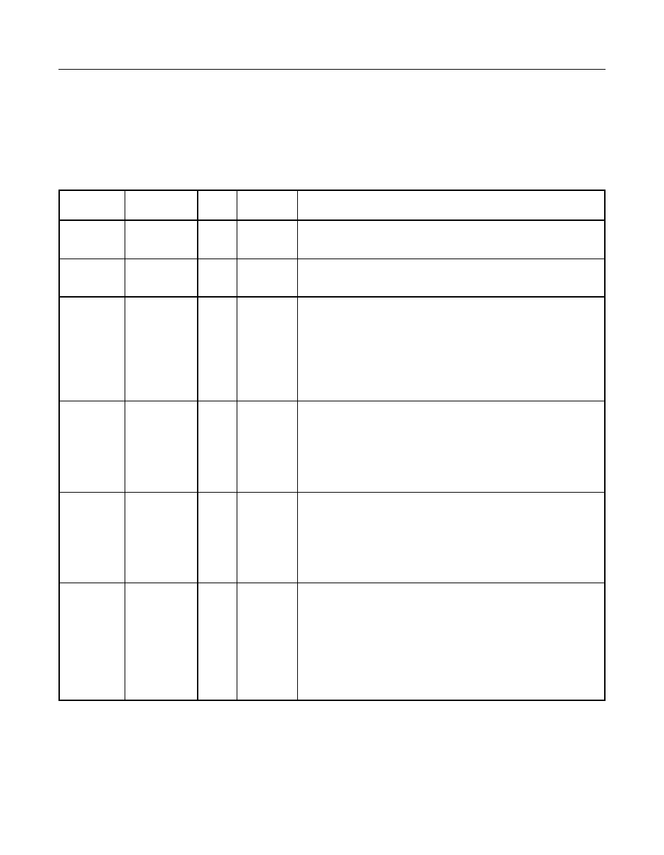
Table 3.15
Flash ROM and Memory Interface Signals
Name
Bump
Type
Strength
Description
MWE/
AC19
O
4 mA
Memory Write Enable. This pin is used as a write
enable signal to an external flash memory.
MCE/
AA18
O
4 mA
Memory Chip Enable. This pin is used as a chip enable
signal to an external EPROM or flash memory device.
MOE/_
TESTOUT
Y18
O
4 mA
Memory Output Enable. This pin is used as an output
enable signal to an external EPROM or flash memory
during read operations. It also tests the connectivity of
the LSI53C896 signals in the “AND-tree” test mode. The
MOE/_TESTOUT pin is only driven as the test out
function when the ZMODE bit (
,
bit 7) is set.
MAS0/
AC18
O
4 mA
Memory Address Strobe 0. This pin latches in the least
significant address byte (bits [7:0]) of an external
EPROM or flash memory. Because the LSI53C896
moves addresses eight bits at a time, this pin connects
to the clock of an external bank of flip-flops which
assemble up to a 20-bit address for the external memory.
MAS1/
AA17
O
4 mA
Memory Address Strobe 1. This pin latches in the most
significant address byte (bits [15:8]) of an external
EPROM or flash memory. Because the LSI53C896
moves addresses eight bits at a time, this pin connects
to the clock of an external bank of flip-flops which
assemble up to a 20-bit address for the external memory.
MAD[7:0]
Y19, AA19,
AC20,
AB20,
AA20,
AC22,
AB21,
AC23.
I/O
4 mA
Memory Address/Data Bus. This bus is used in
conjunction with the memory address strobe pins and
external address latches to assemble up to a 20-bit
address for an external EPROM or flash memory. This
bus puts out the least significant byte first and finishes
with the most significant bits. It also writes data to a flash
memory or read data into the chip from external
EPROM/flash memory. These pins have static pull-downs.