Scsi test four (stest4), Register: 0x52, Register: 0x53 – Avago Technologies LSI53C896 User Manual
Page 212
4-100
Registers
Version 3.3
Copyright © 1998–2003 by LSI Logic Corporation. All rights reserved.
Register: 0x52
SCSI Test Four (STEST4)
Read Only
SMODE[1:0]
SCSI Mode
[7:6]
These bits contain the encoded value of the SCSI
operating mode that is indicated by the voltage level
sensed at the DIFFSENS pin. The incoming SCSI signal
goes to a pair of analog comparators that determine the
voltage window of the DIFFSENS signal. These voltage
windows indicate LVD, SE, or HVD operation. The bit
values are defined in the following table.
LOCK
Frequency Lock
5
This bit is used when enabling the SCSI clock quadrupler,
which allows the LSI53C896 to transfer data at Ultra2
SCSI rates. Poll this bit for a 1 to determine that the clock
quadrupler has locked to 160 MHz. For details on
enabling the clock quadrupler, refer to the descriptions of
, bits 2 and 3.
R
Reserved
[4:0]
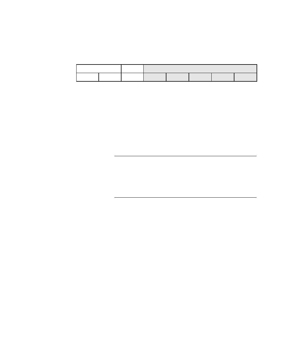
Register: 0x53
Reserved
7
6
5
4
0
SMODE[1:0]
LOCK
R
0
0
0
0
0
0
0
0
Bits [7:6]
Operating Mode
00
Not Possible
01
HVD or powered down (for HVD mode, the
DIF bit must also be set)
10
SE
11
LVD SCSI