Memory read or write, Figure 5, Instruction op code fetch – Zilog Z08470 User Manual
Page 21: Figure 5 d
UM008007-0715
Memory Read Or Write
Z80 CPU
User Manual
9
Memory Read Or Write
Figure 6 shows the timing of memory read or write cycles other than an op code fetch
cycle. These cycles are generally three clock periods long unless wait states are requested
by memory through the WAIT signal. The MREQ signal and the RD signal are used the
same way as in a fetch cycle. In a memory write cycle, the MREQ also becomes active
when the address bus is stable so that it can be used directly as a chip enable for dynamic
memories. The WR line is active when the data on the data bus is stable so that it can be
used directly as a R/W pulse to virtually any type of semiconductor memory. Furthermore,
the WR signal goes inactive one-half T state before the address and data bus contents are
changed so that the overlap requirements for almost any type of semiconductor memory
type is met.
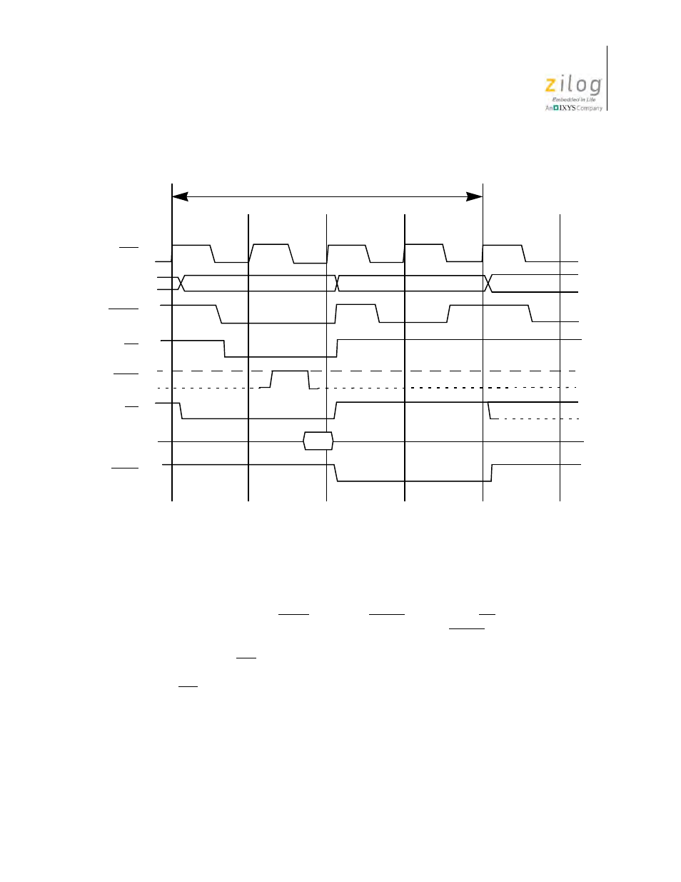
Figure 5. Instruction Op Code Fetch
PC
Refresh Address
M1 Cycle
CLK
MREQ
RD
WAIT
M1
RFSH
IN
D7–D0
A15 –A0
T2
T4
T1
T1
T3