Verilink PRISM 3030 (34-00208.L) Product Manual User Manual
Page 89
79
Table A-3 V.35 Interface Specifications
Characteristics
Specifications
Balanced Drivers
Voltage Swing
±
0.55 V (
±
20%) into
100
Ω
resistive load at
< 0.2 VDC offset
Source Impedance
50
Ω
(
±
10%)
Rise Time
±
10% of UI to
minimum of 40 ns
Balanced Receivers
Load Impedance
100
Ω
(
±
10%)
Resistance from shorted
terminals to ground
150
Ω
(
±
10%)
Differential Input Voltage
>
±
0.2V
Unbalanced Drivers (RS-232/V. 28)
Output Voltage
10.0 V peak (
±
0.5 V)
Output Impedance
300
Ω
minimum
Slew Rate
30 V per
µ
sec maximum
Short Circuit Current
12 mA maximum
Mark Voltage (1 or Off)
0.0 V maximum
Space Voltage (0 or On)
+ 5.0 V minimum
Unbalanced Receivers (RS-232/V.28)
Input Voltage
±
25 V maximum
Load Impedance
3000
Ω
– 7000
Ω
Mark Voltage (1 or Off)
0.0 V maximum
Space Voltage (0 or On)
+ 2.0 V minimum
A
C
D
E
K
L
F
H
J
P
R
U
Y
Z
V
T
X
M
N
S
W
AA
BB
CC
DD
EE
FF
HH
JJ
KK
LL
NN
MM
B
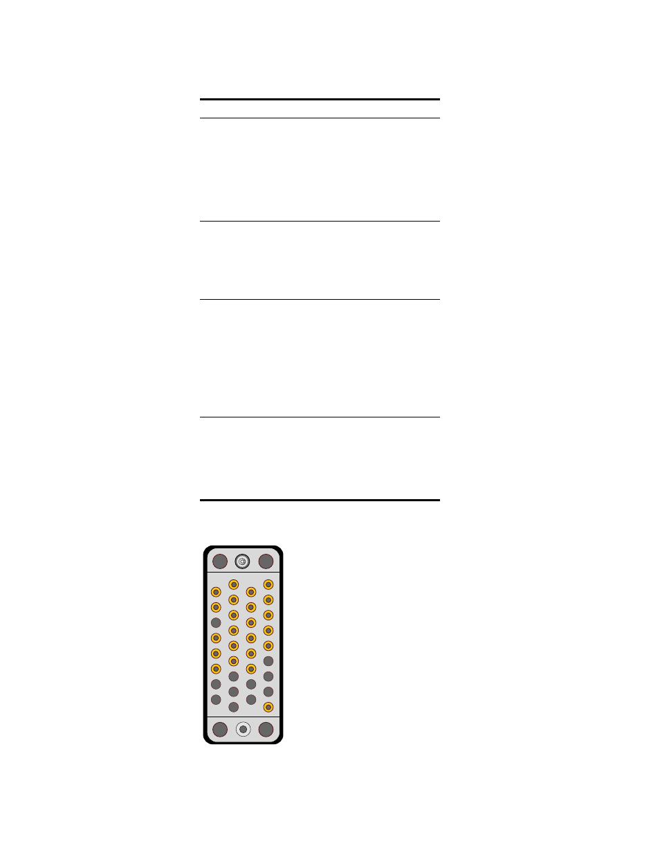
Figure A-1 Winchester-type Connector