Table 2–5, Creating an emulated – Altera External Memory PHY Interface User Manual
Page 13
Chapter 2: Parameter Settings
2–7
© January 2010
Altera Corporation
External Memory PHY Interface (ALTMEMPHY) (nonAFI) Megafunction User Guide
Creating an Emulated x36 QDR II+/QDR II SRAM ALTMEMPHY Variation
From software implementation point of view, creating a ×36 emulated QDR II+/QDR
II SRAM interface is exactly the same as implementing an interface with two ×18
QDR II+/QDR II SRAM devices. In the Memory Settings page of the ALTMEMPHY
MegaWizard interface, select a ×18 QDR II+/QDR II SRAM with the same timing
specifications as ×36 QDR II+/QDR II SRAM device (see
).
For more information about ×36 emulation for QDR II+/QDR II SRAM interfaces,
refer to the Exceptions for ×36 Emulated QDR II and QDR II+ SRAM Interfaces in Arria II
GX, Stratix III and Stratix IV Devices sect
External Memory Interface Handbook.
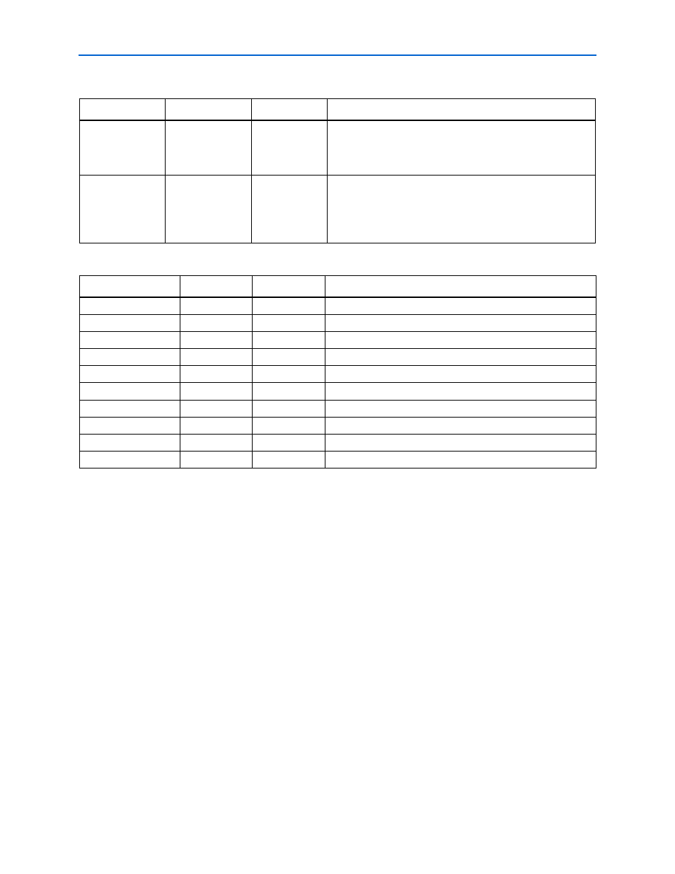
Table 2–4. QDR II+/QDR II SRAM Initialization Options
Parameter Name
Range
Units
Description
Memory burst
length
4
beats
Sets the memory burst length for the interface. As the
QDR II+/QDR II SRAM ALTMEMPHY megafunction only
supports half-rate designs, only a memory burst length of four
is supported, which equates to a local burst length of one.
Memory latency
setting
1.5 (QDR II
SRAM) or 2.5
(QDR II+ SRAM)
Cycles
Sets the memory latency. Altera devices only support latency of
2.5 for QDR II+ SRAM and 1.5 for QDR II SRAM. QDR II+
SRAM with latency of 2.0 is not supported with Altera devices,
even though the ALTMEMPHY MegaWizard interface shows
this as an option.
Table 2–5. QDR II+/QDR II SRAM Timing Parameter Settings
Parameter Name
Range
Units
Description
t
SA
200–500
ps
Address setup time to K clock rise.
t
SC
200–500
ps
Control setup time to K clock rise.
t
HA
200–500
ps
Address hold time to K clock rise.
t
HC
200–500
ps
Control hold time after K clock rise.
t
SD
200–500
ps
D setup time to K clock rise.
t
HD
200–500
ps
D hold time to K clock rise.
t
CQHQV
200–500
ps
Echo clock high to data valid.
t
CQHQX
200–500
ps
Echo clock high to data invalid.
t
CQHCQnH
0–2,000
ps
Echo clock high to inverted echo clock high.
t
CQH
0–2,000
ps
Echo clock high.
Note to
(1) This parameter is available for QDR II+ SRAM interfaces only.