Qdr ii+/qdr ii sram signals, Qdr ii+/qdr ii sram signals –20, Table 3–10 – Altera External Memory PHY Interface User Manual
Page 36
3–20
Chapter 3: Functional Description—ALTMEMPHY (nonAFI)
ALTMEMPHY Signals
External Memory PHY Interface (ALTMEMPHY) (nonAFI) Megafunction User Guide
© January 2010
Altera Corporation
shows additional calibration status signal outputs from the sequencer. You
can either pull these signals out to the top level or observe them through the
SignalTap
®
II logic analyzer.
QDR II+/QDR II SRAM Signals
This section describes the ALMEMPHY megafunction signals for QDR II+/QDR II
SRAM.
through
show the signals.
1
Signals with the prefix mem_ connect the PHY with the memory device; signals with
the prefix ctl_ connect the PHY with the controller.
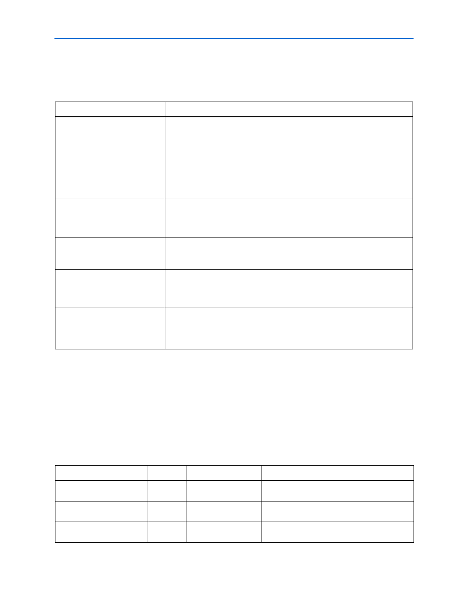
Table 3–10. Additional Calibration Status Signals—nonAFI
Signal
Description
rsu_codvw_phase
(Center of data valid window)
The ALTMEMPHY resynchronization setup unit (RSU) sweeps the phase of a
resynchronization clock across 360° (full-rate designs) or 720° (half-rate designs) of
a memory clock cycle. Data reads from the DIMM are performed for each phase
position and a data valid window is located, which is the set of resynchronization
clock phase positions where data is successfully read. The final resynchronization
clock phase is set at the center of this range: the center of the data valid window
(CODVW). This output is set to the current calculated value for the CODVW and
represents how many phase steps were performed by the PLL to offset the
resynchronization clock from the memory clock.
rsu_read_latency
(Read latency at the center of the
window)
If the RSU can find one data valid window (and not more than one), the
resynchronization clock is positioned at the center and the rsu_read_latency
output is then set to the read latency (in phy_clk cycles) using that
resynchronization clock phase. If calibration is unsuccessful, this signal remains at 0.
rsu_no_dvw_err
(Calibration failed due to no window
found)
If the RSU sweeps the resynchronization clock across every phase and does not see
any valid data at any phase position, calibration fails and this output is set to 1.
rsu_grt_one_dvw_err
(Calibration failed due to more than
one valid window)
If the RSU sweeps the resynchronization clock across every phase and sees multiple
data valid windows, this indicates unexpected read data (random bit errors) or an
incorrectly configured PLL, which must be resolved. Calibration has failed and this
output is set to 1.
rsu_multiple_valid_
latencies_err
(Calibration failed due to more than
two read latencies)
If the RSU sweeps the resynchronization clock across every phase and sees valid
data at more than two different latencies, calibration fails and this output is set to 1.
Table 3–11. I/O Interface to QDR II+/QDR II SRAM
(Part 1 of 2)
Signal Name
Type
Width
Description
mem_addr
output
MEM_IF_ROWADDR_
WIDTH
Memory address bus.
mem_clk
output
MEM_IF_CLK_PAIR
_COUNT
Memory clock, positive edge clock (K).
mem_clk_n
output
MEM_IF_CLK_PAIR
_COUNT
Memory clock, positive edge clock (K#) 180° offset
from mem_clk.