Altera External Memory PHY Interface User Manual
Page 67
Chapter 3: Functional Description—ALTMEMPHY (nonAFI)
3–51
Design Considerations
© January 2010
Altera Corporation
External Memory PHY Interface (ALTMEMPHY) (nonAFI) Megafunction User Guide
string EXT_SELECT, an extra cycle of latency can be dynamically inserted on the
address and command outputs by asserting the ctl_add_1t_ac_lat input. This
allows run-time control of the address and command latency. If ADDR_CMD_ADD_1T
is set to the string value TRUE, the extra clock cycle of latency is always present, and
if it is set to the string value FALSE, the extra latency is never added.
1
The ADDR_CMD_ADD_1T parameter value is set in <variation_name>_phy.v file and is
passed on to <project directory>\<variation_name>_alt_mem_phy.v file.
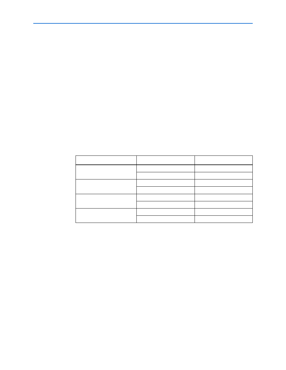
For DDR2 SDRAM interfaces using unbuffered DIMMs or components, the value of
ADDR_CMD_ADD_1T
should be TRUE for odd CAS latencies (CL3 or CL5) and FALSE
for even CAS latencies (CL4). For registered DIMMs, the value of ADDR_CMD_ADD_1T
should be FALSE for odd CAS latencies (CL3 or CL5) and TRUE for even CAS
latencies (CL4), see
.
For DDR SDRAM interfaces, the write latency is fixed at one cycle. You should use the
settings for CAS latencies see
shows the setting of ADDR_CMD_ADD_1T for different values of CAS
latency and DIMM settings.
The timing of the ODT signal can be controlled in the same way but is independent of
the address and command latency. If the ODT_ADD_1T parameter is set to
EXT_SELECT
, an extra cycle of latency can be dynamically inserted on the ODT
command outputs by asserting the ctl_add_1t_odt_lat input. This allows
separate run-time control of the latency of the ODT signal. If ODT_ADD_1T is set to
TRUE
, the extra clock cycle of latency is always present. If ODT_ADD_1T is set to
FALSE
, the extra latency is never added.
Table 3–18. ADDR_CMS_ADD_1T Settings
Memory and CL
DIMM Type
ADDR_CMD_ADD_1T
DDR2 SDRAM, CL3
Unbuffered
TRUE
Registered
FALSE
DDR2 SDRAM, CL4
Unbuffered
FALSE
Registered
TRUE
DDR2 SDRAM, CL5
Unbuffered
TRUE
Registered
FALSE
DDR SDRAM
Unbuffered
FALSE
Registered
TRUE