Altera External Memory PHY Interface User Manual
Page 15
Chapter 2: Parameter Settings
2–9
© January 2010
Altera Corporation
External Memory PHY Interface (ALTMEMPHY) (nonAFI) Megafunction User Guide
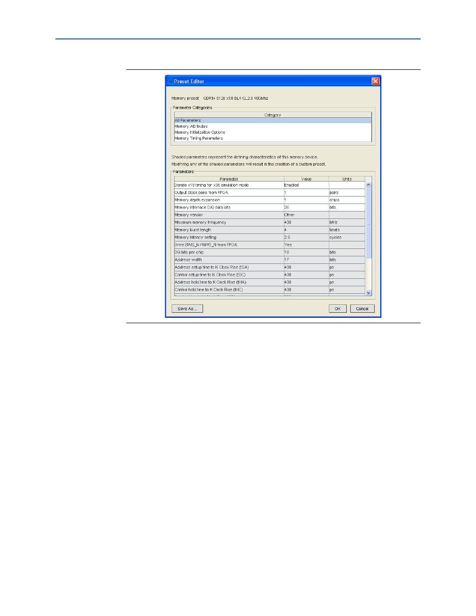
2. For Derate ×18 timing for ×36 emulation mode, select Enabled. This setting tells
the report_timing.tcl script to use the derating factor for ×36 emulation. If you
have modified the board such that the slew rate of the ×36 emulated (double-
loaded) CQ/CQn signal is comparable to a non-emulated (single-loaded)
CQ/CQn signal, you can leave this option as Disabled, as there is no slew rate
degradation in your design.
3. For Output clock pairs from FPGA select 1. Only one mem_clk and mem_clk_n
pair connect to the QDR II+/QDR II SRAM device's K and Kn ports..
4. Memory interface D/Q data bits select 36, which is the data bus width for ×36
QDR II+/QDR II SRAM interfaces.
After generation, for devices with F780 and F1152 packages that do not have ×18 DQ
groups necessary to fit the write data bus, follow these steps to modify the
<variation_name>_pin_assignments.tcl file to change the assignments to use ×9 DQ
groups:
1. Remove the memory interface data pin group assignment of 18 for write data bus
and DM pins in the Assignment Editor.
2. Find the following assignments in the <variation_name>_pin_assignments.tcl.
set_instance_assignment -name MEMORY_INTERFACE_DATA_PIN_GROUP 18 -to
${d_pin_name}\[0..17\] -from ${d_pin_name}\[0\]
Figure 2–4. Preset Editor